Looking at the huge gap between the revenue of semiconductor design and manufacturing (~$300B) and that of EDA tools, services and silicon IP combined (~6B) inspired me to look more deeply into the overall arena of semiconductors in today’s context and possibly decipher some trends which should emerge in near future. Although this gap in revenue always existed, in the realm of SoCs and ever increasing complexity on a single wafer over last few years, the gap seems to be justified and may open up new chapters in the semiconductor arena. I have been watching the developments in this space for a few years and the industry seems to be at an inflexion point. This prompted me to write this article.
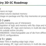
In the backdrop of ever increasing demand for higher density at lower nodes, thereby increasing most intricate design and process rules and manufacturability, it is evident that designs need to be much closer to manufacturing. Some of this is being addressed by semiconductor IPs which are specialized components targeted at particular nodes. Possibly due to this, the IP business has increased to much extent, rightly pointed by Eric Esteve in his Jan 2012 article, that Q311 silicon IP revenue ($568M) has surpassed the overall revenue of CAE ($566M). With the geometry reduction, power became critical which took the front seat thus giving rise to High K metal gate and vertical gate or FinFET transistors in technology and several CAE techniques such as concept of power domain over clock gating and so on. There are other manufacturing complexities, e.g. reducing metal pitch giving rise to coupling effects and signal integrity issues, at 20nm and below this asks for double and higher patterning technique which in turn asks for new routers to accommodate different masks for the same layer. After all one common theme emerging is that lower geometry (20nm and below) made to work can give rise to large saving in area and power as well as can provide very high speed. For increasing capacity and possibly reducing assembly complexity, 3D ICs are on the horizon.
Now let us look at the economic and business scenario in this arena. Foundries have led the way for semiconductor technology development, so definitely they need to be the largest share holders. Then comes some of the dominant application players, wireless is the largest growing and in that market Qualcomm is the giant with huge cash reserves. However, Qualcomm does not have a foundry and hence it has to share its profit margin with foundry. Samsung has its presence in home appliances, entertainment, and smart phone and so on. Then there are memory and storage players like Micron and ST. A very important, Silicon IP is an element spread across everywhere with ARM being a dominant player in that space. Then there is EDA, CAE, serving all of these spaces as per their needs. While large technology advancement has taken place and more is being done, economic pressure has increased. Multiple players have increased in each of these spaces and purchasing power of a consumer has decreased, there by resulting into depressed profit margins, mostly in single digit. Definitely there is a case of consolidation in each of these spaces. What looks to be obvious is that high-end foundries combined with design will be the leader in the overall semiconductor landscape. Following are some of the possible scenarios I can think of –
Foundries – Intel and TSMC will lead the way being ahead in the process node compared to the rest and hence taking advantage of enabling high-end SoCs. Samsung, Global Foundry and SMIC are there to follow.
Appliances, Storage – Home appliances, automotive, Entertainment – Samsung, Micron, and ST will remain the leaders.
Wireless and mobile application – Qualcomm will continue to lead the way. It needs to find the way to reduce or eliminate margin paid to the foundry and that could bring a large surprise considering the money power Qualcomm has.
Semiconductor IP – This is a brain child which will continue growing in design IP space. The processor dominant, ARM can grow further and communication IP player Qualcomm will continue growing. Other IP players can consolidate with ARM and Qualcomm.
EDA – Synopsys, Cadence and possibly Mentor will continue their lead in EDA tools space. Quite often it has been felt that an EDA company should get a share in the chip produced by its tool. However the important point to note here is that an EDA company does not provide any design IP, it provides tools which get driven by the foundry requirements. Hence in broader sense EDA is a service to foundry, the new technology in foundry drives the enhancements into EDA tools to cater to those needs or accommodate them. Moreover in SoC age, the design is more and more IP and foundry driven. It makes sense for EDA tools to work in association with foundries. When foundries will consolidate, then it will not be a surprise if major players like Intel and TSMC acquire big EDA players like Synopsys, Cadence and Mentor.
I did not talk about computing space, PC, notebook etc. With the arrival of iPad and mediaTablet, that space will be led by the experts like Apple, Intel, and IBM and so on. Of course in the overall eco system and design chain, there will remain multiple players in every domain, but they will operate as services to the consolidated giants.