Adding sophisticated 2D dynamic compaction technology to address 20nm and 14nm challenges. Santa Clara, California – May 3 ,2012 – Sagantec today announced that it has acquired Dutch startup NP-Komplete Technologies BV (Eindhoven, The Netherlands) for its physical design compaction and migration solutions based on a sophisticated 2D dynamic compaction technology. NP-Komplete Technologies (NPKT) is a provider of innovative DFM solutions, and physical design optimization engines. Terms of the acquisition are confidential.
Having worked with Sagantec over the years, I can tell you a little more of what is going on here. Sagantec has been leading the process migration march since ~1996. That was some 16 years and 10 semiconductor process nodes ago. During that time Sagantec introduced the industry’s first hierarchical compaction/migration tool, they added Cadence Virtuoso, OpenAccess, and Pcell support, they added analog design constraints, etc… Sagantec actually coined the term “process migration” and made it a viable EDA market segment.
The Sagantec engineering team in the Netherlands is now fully integrated with the NPKT team with the combined team working together on enhancing the tools and addressing future technology challenges.Following the acquisition, NPKT is now a wholly-owned subsidiary of Sagantec and continues to develop and provide advanced layout compaction and DFM solutions.
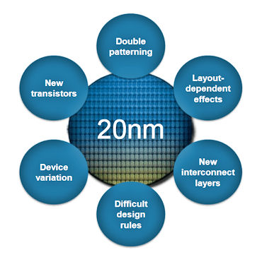
The Eindhoven guys wrote the original Sagantec compactor then re-wrote it for Takumi’s DFM products and later spun out to re-write it again for NKP. This perpetual march down the shrinking geometry path has epitomized our industry since Moore “enacted” his law (observation) in 1965, and this trend is not going to go away anytime soon. However, as dimensions shrink further and deeper, each new technology transition seems to be a little more disruptive than the previous ones, presenting new concepts and more difficult challenges for design rule compliance and layout migration. The current 28nm design rules and evolving 20nm technologies are really complex and hard to manage, so adding some innovation and refreshing the compaction engine will help to solve the 20nm puzzles.
The NPKT migration technology is an automated layout optimization technology, and was designed from the ground up to address the latest challenges of 20nm design rules. Since most of the new rules are enforced to overcome manufacturability-related challenges that impact yield, it takes a sophisticated 2D compaction technology to make necessary modifications to create a DRC clean layout. The NPKT technology has already been proven with DRC clean results at several tier-1 semiconductor companies, and used on multiple 28nm and 20nm technologies of leading-edge foundries. The addition of this new technology and expertise enables Sagantec to better address the new challenges and overcome technology discontinuities that result from the introduction of new layers and new types of design rules associated with the 20nm process node while producing best possible quality results.
Sagantec will have this and other innovative technologies at the Design Automation Conference in San Francisco next month. Even more importantly, Sagantec will have me in their booth talking about the challenges of 20nm and how the fabless semiconductor ecosystem will continue to thrive in the coming process nodes. See you there!