This is the eighth in the series of “20 Questions with Wally Rhines”
In 1972, I joined TI and was assigned to work on a new contract that had just been awarded and badly needed staffing. The U.S. Department of Defense had decided that solid-state charge-coupled device (CCD) image sensors were going to be a strategic technology and they formed a joint services program under Larry Sumney (who later became CEO of the Semiconductor Research Corporation for more than thirty years). Fairchild had hired Gil Amelio from Bell Labs and was promoting buried channel technology because of its high efficiency, i.e., by using ion implantation to shift the minimum of the electrical potential to store charge below the surface of the silicon, any losses due to surface state interactions were minimal. Meanwhile, RCA was a clear contender in this emerging business because of their experience with video cameras and associated technology (as was Sony, but Sony could not be funded by the U.S. DoD).
 TI was desperate to be included in the contract shootout, so they proposed a totally different approach, building the CCD on a silicon wafer and then thinning the devices from the back side to about a 25-micron thickness. This approach avoided the losses associated with shining light on the front side of the device where polysilicon and metal interconnect interfered with light transmission. The CCD thinning technology was relatively simple. We used wafers with a 25-micron thick, lightly doped p-type epitaxial layer on top of a heavily p+ doped substrate. The p-layer served as an etch stop leaving the 25-micron paper-thin layer. TI’s proposal looked good to the Navy’s Night Vision Lab for use in “Starlight Scopes” and, at the last minute, TI was added to the contract. Today, virtually all solid-state imagers are illuminated from the back side of the silicon but that approach really didn’t take off for thirty more years.
Meanwhile, Dean Collins, who ran the CCD Imaging Branch was able to promote the technology to other branches of the government, and lots of additional funding was generated for TI. One particularly difficult contract called for building a moving target indicator that would store and compare successive images. Larry Hornbeck took on the task but stubbornly refused to fabricate the device as originally proposed. Instead, he pursued what he called a stratified channel CCD architecture, the first-ever CCD to have the capability for storing two overlying charge-storage and transport channels. With the assistance of people like Ken Bean (discussed in the last blog) for the epitaxial process development and Jerry Hynecek (inventor of TI’s virtual-phase CCD) for the modeling task, Larry proved the concept with backside illumination of thinned, packaged devices.
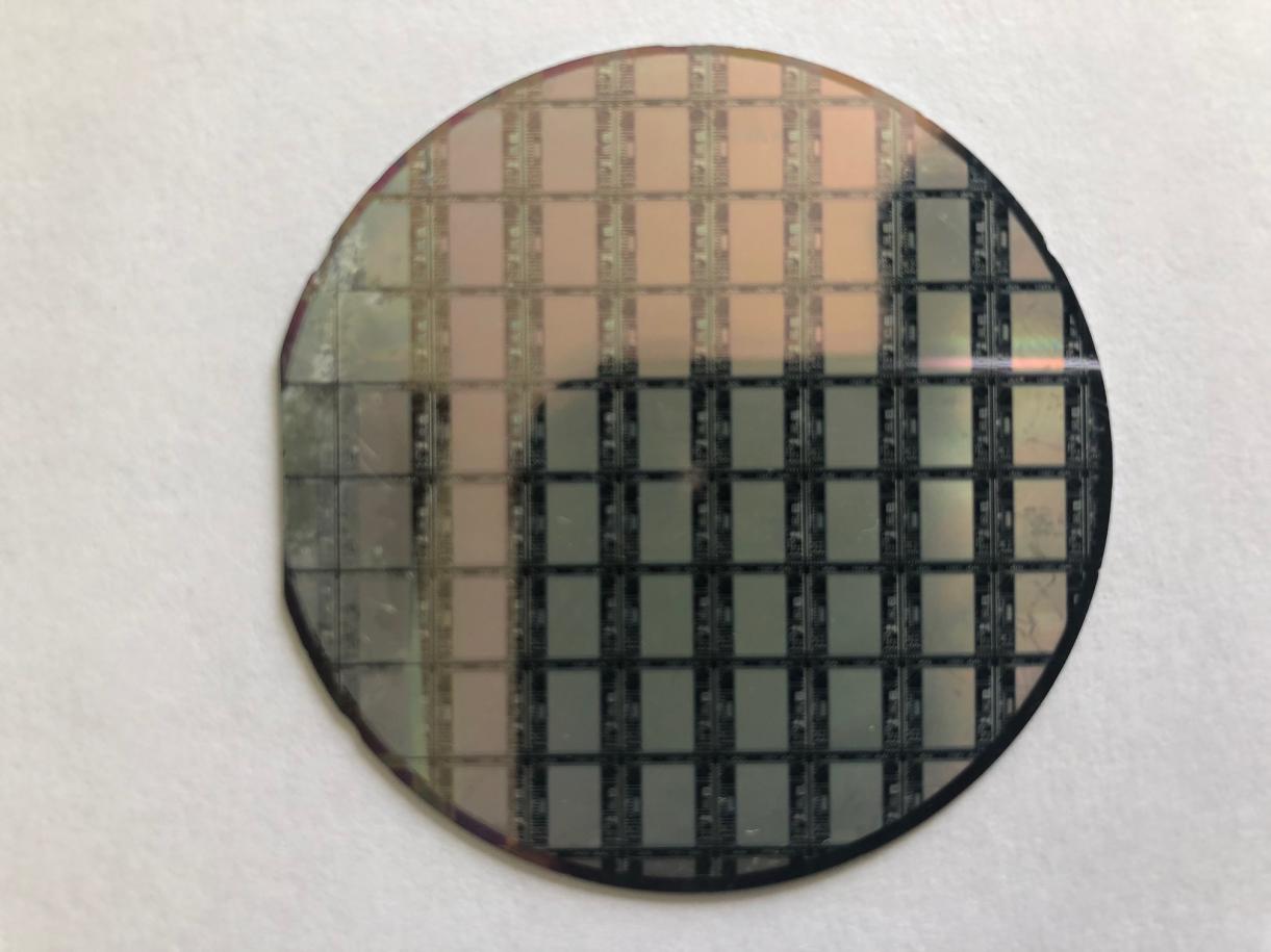
Dean sold another program to the DoD, this time for a “solid state light modulator” that again relied on TI’s thinning expertise. It used a hybrid manufacturing process to produce a frontside, deformable mirror spatial light modulator, with backside CCD-addressing. The deformable mirror was a continuous sheet of a metalized polymer membrane. Once again, Larry came up with a different approach, consistent with his future habit of taking on the management to pursue approaches that ultimately proved to be superior and more manufacturable on the path to his “Digital Micromirror Device” or DMD. Larry was convinced that creating arrays of individually-addressable cantilever micromirrors along with a monolithic manufacturing process would solve problems of defects in the array and lead to much improved optical performance. By this time, I had taken on the job of President of the Data Systems Group and Tom Stringfellow, who managed the Peripheral Products Division of the Group, began funding Ed Nelson to support a potentially revolutionary approach to printing using the digital micromirrors. George Heilmeier, who was one of the first senior TI managers to be hired from outside the company, became VP of Research for TI and supported Larry for the chip development. By 1986 Larry had developed and patented the first practical methods for manufacturing high-density arrays of micromirrors on an integrated circuit in a conventional wafer fab. This IP and its sound reduction to practice by Larry served as an initial barrier to potential competitors who would have immediately started developing their own version of the digital micromirror device, once it was publicly disclosed in 1988. Thirty-one years after the invention of the digital micromirror device in 1987, TI is still the only manufacturer of this disruptive technology, a highly unusual, and possibly unique, example in semiconductor history.
Larry made a pivotal decision in 1987 to attach the micromirrors to torsional suspensions and actuate them into contact with rotation stops. This made it possible to manipulate light with the precision of time division by pulse-width modulation, increased the optical efficiency and reduced the address voltage. And so, the digital micromirror device (also DMD) was born (U.S. Patent 5,061,049, Spatial Light Modulator and Method, Inventor L.J. Hornbeck). The DMD became commercially known as the DLP chip.
The tiny mirrors of this device assumed a “1” or “0” position and pulse width modulation was applied to control the pixel intensity, a method that required extensive algorithmic development to produce high quality projected images. Numerous other problems had to be solved, such as the gradual increase in surface stiction to the point where a mirror would stick in a “1” or “0” position, a problem Larry immediately addressed with a novel, electro-mechanical release mechanism and in 1990 with a surface treatment that he developed (despite his claim that he hated chemistry).
Through all this, the Semiconductor Group didn’t want to take the product to production. Potential applications, like projection TV, would require major investments with questionable business benefit since the light modulator component was a small part of the total system cost. But TI, with some government help, provided enough funding to keep it alive and Larry’s persistence provided the momentum.
And then, in the late 1980s, Jerry Junkins became CEO of TI. Jerry was looking for a semiconductor project with system implications that could make a real difference to the company. Jerry’s background was running the defense business of TI and the DMD looked good to him. So, he redirected the staff of an older (four inch) wafer fab that was destined to be shut down and totally dedicated it to working out the bugs in the DLP chip.
TI built a total portfolio of know-how, software, CMOS-based manufacturing technology and intellectual property to lock up an amazingly disruptive technology. The entire motion picture industry distribution structure was totally changed as its 115 year old projection systems were replaced by “DLP Cinema” technology and software based distribution of motion pictures. TI approached other applications including printing and home projection systems with a solutions approach that included the basic DLP component, algorithmic development, manufacturing, and application engineering. The revenue approached $1B, and companies like Samsung and RCA introduced televisions based upon the DLP because of its extremely bright, sharp colors.
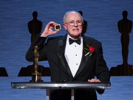
Ultimately, Larry Hornbeck, the innovator and developer of the technology, was nominated for and received an Academy Award of Merit (Oscar statuette) in 2015. Most interesting to me, however, is the fact that TI kept the DLP program alive for almost twenty years before any real revenue was realized. This wasn’t the only example of persistence at TI, accompanied by tolerance for inflexible innovators, and it is part of the reason that TI is the only semiconductor company that has ranked among the ten largest since the 1950s.
The 20 Questions with Wally Rhines Series
Share this post via:


Silicon Insurance: Why eFPGA is Cheaper Than a Respin — and Why It Matters in the Intel 18A Era