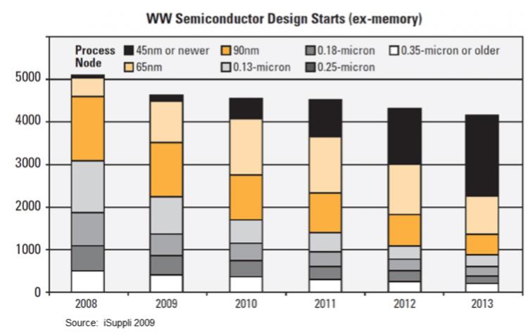
 Analog has always been difficult, a bit of a black art persuading a digital process to create well-behaved analog circuits, capacitors, resistors and all the rest. In the distant past, we would solve this by putting the analog on a separate chip, often in a non-leading-edge process. But modern SoCs integrate large amounts of digital logic along with RF, analog and mixed-signal functionality on a single SoC and then manufacture it in the most bleeding edge process. This is a huge challenge.
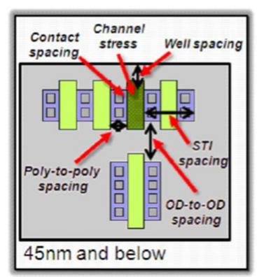
The complexity of design rules when you get down to 28nm and below has greatly complicated the process. Traditionally custom layout is tedious and inflexible once started (you only have to think of the layout impact of a trivial digital gate-level change to see this). As a result, the layout teams don’t start layout until the circuit design is nearly complete and so they have to work under tremendous tape-out pressure. However, a more agile approach is possible using automated efforts. These reduce the effort needed, allow layout to be overlapped with circuit design and produce better (specifically smaller) layouts.
 Timely design of the RF, analog and mixed-signal parts of many SoCs has become the long pole in the tent, the part of the schedule driving how fast the chip can be taped out. Part of the challenge is technical since the higher variability of silicon in 28mm and below (and above too, but to a lesser extent) threatens to make many analog functions unmanufacturable. To cope with variability and control parasitics, foundries have introduced ever more complex design and DFM rules and designers have come up with ever more elaborate circuits with more devices. Of course, both of these add to the work needed to complete designs.
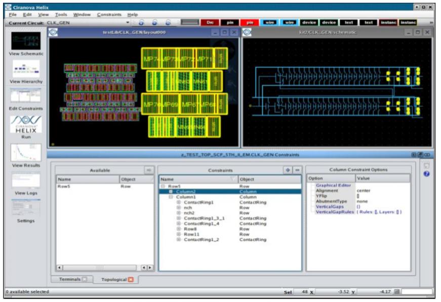
The solution is an agile layout flow involving large-scale automation. The key advance is the capability to quickly lay out not just a single structure (e.g. a current mirror) in the presence of a few localized rules, but rather the entire design hierarchy in the presence of all the rules (complex design rules, area constraints, signal flow, matching, shielding etc).
Only by automating the whole layout process is it possible to move to an agile “throw away” layout to be done before the circuit design is finalized, and thus start layout earlier and do it concurrently with circuit design.

The advantages of this approach are:
- significantly lower layout effort, since tasks are automated that were previously done by hand. This is especially the case in the face of very complex design rules where multiple iterations to fix design rule violations are avoided
- large time-to-market improvement since the design is started earlier and takes less total time, so finishes soon after circuit design is complete
- typically, at 28nm, a 10-20% die size reduction versus handcrafted layout
For more details of Ciranova’s agile layout automation, the white paper is here.
Share this post via:


Captain America: Can Elon Musk Save America’s Chip Manufacturing Industry?