The problem:To move dual-port SRAM library and macros from a 40nm process to a 28nm process. In addition to all the changes between two different foundry processes, the 28nm rules are disruptive and incompatible with the previous rules. The memory corecells (foundry-specific) would also need to be completely replaced.
Current wisdom was that an IP block migration to 28nm was impossible and a complete re-design would be required. As usual, the schedule was very aggressive so a quick migration was really the only feasible option.
The main changes: There were many changes in design rules between the two foundry processes. Some of the most challenging changes were:
- No poly bends. The original process allowed poly bends and made extensive use of them in the design.
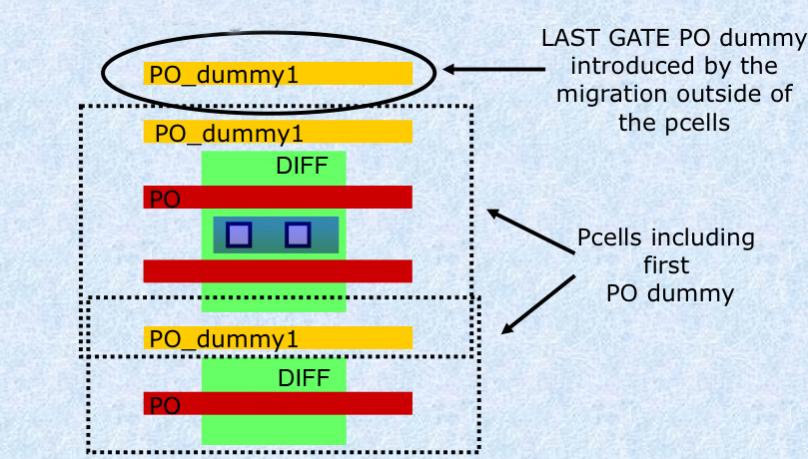
- Extra dummy rule. Small transistor stacks required an additional dummy poly “gate” off the end of the transistor. This was not electrically functional, but was required for optical lithography reasons.
- Memory core cells from the original process were replaced with new core cells for the new process. These new core cells are architecturally different, resulting in various mismatches that would require attention.
- ]Devices outside the memory core-cells needed to have width and length adjusted according to complex rules.
- ]All devices must be vertical. The original design was done in the horizontal direction meaning it must be rotated when it is written onto the reticle.
The main non-changes: Many aspects of the design could not be changed. The design was originally done using Virtuoso and Pcells in DFII but the migrated design needed to be in OpenAccess. It was important to maintain the hierarchy and ensure that LVS would pass for the new design. Transistor aspect ratios also needed to be adjusted appropriately.
The schedule: There was only a month to do the migration. No more than two days of manual cleanup was allowed at the end to fix anything that could not be migrated automatically.
How each major challenge was addressed:
No poly bends. When possible, the poly would need to be replaced with metal1 if the routing channel was open. If the routing channel was not open, then the result was left LVS clean but with DRC violations that would need to be fixed manually. A preliminary analysis revealed that there would be very few such cases left.

To avoid poly bend violations, the tool automatically moved poly/metal connections in cases it was needed to keep the poly line straight.

Extra dummy rule. The extra dummy rule requires that additional dummy poly “gates” are added to the end of transistors below a certain size. This is complicated by the fact that the transistors appear within Pcells.
Memory core cells. The memory core-cells from the original design were replaced with new foundry-provided core-cells for the new target process. A direct mapping was possible for most of the core cells including abutments that could be handled directly.
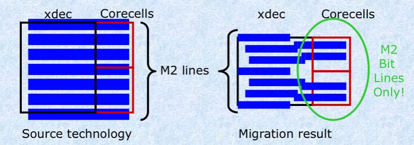
However, the mapping of interconnections between the core cell array and the decoders and I/Os were another challenge. There were fewer horizontal metal2 lines in the new technology and so the number of lines had to be adjusted during the migration.
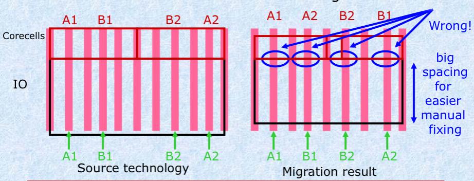
Similarly there were a different number of metal3 lines which required adjustment during the migration. Further, the metal3 lines needed to be re-ordered (the order that they emerged from the core was different for the two architectures). The re-ordering of lines had to be done manually after the migration but space was automatically left to make this straightforward.
Device resizing. Transistors needed to be re-sized automatically during the migration according to complex rules. Devices with channel length of 40nm were mapped to 30nm. Longer channel devices had their channel length shortened to a certain specific ratio of the original length. As for transistor channel widths, these were shrunk by different ratios for the nMOS vs. the pMOS transistors. The minimum width was further constrained to a specific size that would force every source/drain to have a minimum of two contacts, for reliability reasons. Clearly, different ratios and limits could have been handled automatically too.
All devices must be vertical. Since the design would be rotated after migration, all design rules needed to interchange horizontal and vertical between the design rule manual and the Sagantec technology file.
Results: The migration was done in three steps.
Step 1: the design rules were encoded into a Sagantec technology file, taking into account the horizontal/vertical interchange.
Step 2: the core-cell array was migrated, taking into account the shrink and the reduction in the number of metal2 lines available. Abutments were all fully respected. The corecell to X-decoder metal2 connections were handled completely correctly.
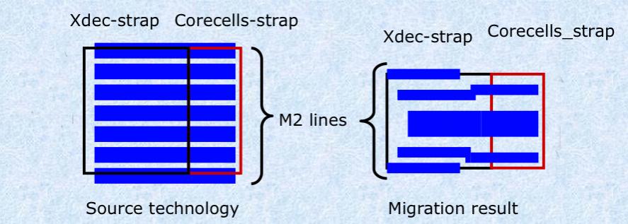
The corecell array to X-decoder-strap was completely handled, including the metal2 lines that could be deleted due to the new abutments.
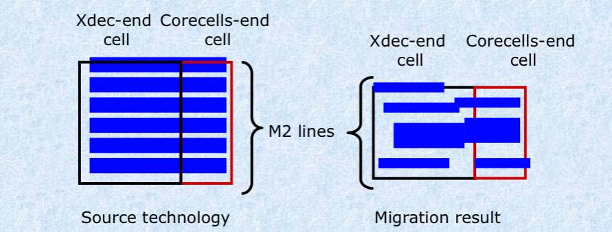
The corecell array to X-decoder end-cell was completely handled correctly.
The core-cell array to I/Os on metal3 was placed completely correctly. However, the order of the lines was incorrect and would need to be fixed manually. Additional space was automatically left to make this task straightforward.
The run time for the entire migration was few hours.
Results: The dual-port SRAM migration was delivered on-time. Minor fixing was required after the initial delivery to update some minor device size changes and other fixes (1½ days in total).
The memory core-cell array was replaced 100% clean. Core cell and peripherals cell placement and abutment was fully respected. Everything except for the re-ordering of I/O lines on metal3 was handled completely automatically.
Devices re-sizing was fully implemented and target devices sizes respected.
As many poly angles were removed as possible. Where this was not possible (since metal1 was already in use) the remaining few violations were left for manual fixing.
The entire project took one man-month (half of that time was spent to set up the design rules and flow from scratch, half to actually perform the migration). A macro 2K by 32 dual-port SRAM macro takes a few hours of run time. Migrating subsequent SRAM instances comes almost free, just a few hours to set up and a few hours of run-time.
IP block migration:Moving a complex custom IP block from one process to a very different process can either be done by an experienced layout team or using an automated flow that handles almost all of the work automatically, such as Sagantec’s migration technology. For migration to older process nodes or between similar processes, it is possible that a shrink followed by manual fix-up of violations would work, but in advanced process nodes and when the processes have different rules, the number of violations generated can be overwhelming and impractical for such approach. The alternative would be a complete redesign, which in this case would be prohibitively expensive in both schedule and resources required. In addition to licensing migration software, Sagantec has also experienced application engineers that can do migrations as a service to minimize turn-around time, get the highest quality results and maximize ROI. In this case study the Sagantec service did not only provide a significant return on the investment, it actually enabled getting these 28nm memory macros implemented in such demanding schedule requirements.

Sagantec Demo Suite Registration


Captain America: Can Elon Musk Save America’s Chip Manufacturing Industry?