 As I have mentioned before, you can tell al lot about a company by their CEO. The previous trip I made to Taiwan was with Helic co-founder and CEO Dr. Yorgos Koutsoyannopoulos. One of the benefits of my job is I get to spend time with some very interesting people from around the world and this was no exception.
Prior to founding Helic, Yorgos worked as a research engineer of ICCS (an academic institute in Athens), in technology development projects for European corporations such as ST Microelectronics, Atmel-ES2 and Infineon. He received his Ph.D. and Diploma in Electrical Engineering from the National Technical University of Athens and he has attended executive courses on leadership and marketing at LBS and Harvard. Yorgos is a well-rounded guy and very personable, and a pleasure to work with.
Helic is an EDA specialist developing innovative and disruptive design automation technologies for the semiconductor market. Founded in May 2000, the company is backed by strategic and venture capital investors including the legendary Andy Bechtolsheim, Synopsys (formerly Magma), and Fujitsu. Helic reaches its customers with a business model combining EDA tools, IP and services, with a mission to enable first-pass silicon while greatly shortening the development cycles of high-speed digital, analog RF and millimeter-wave ICs.
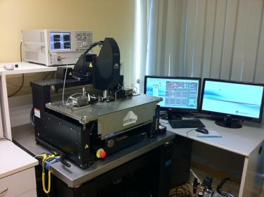
 Helic has more than 60 corporate customers and more than 1,500 users who design chips for a wide range of applications; from cellphone standards (1-2.1GHz), Bluetooth and WiFi (2.4-5.8GHz) to Gbit Ethernet, to multi-core CPUs and GPUs and to mm-wave applications. Helic is also the only emerging EDA company that I know of that has a full silicon correlation lab to perform on-chip measurements up to 70GHz.
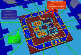
Helic’s background technology is a unique high-speed parasitics extraction methodology. It was conceived to address a critical missing link in custom IC design flows and accelerate the development of complex RFICs and systems-in-package by enabling rapid, whole-chip electromagnetic modeling early in the design flow. The technology has been in use since 2000 by fabless companies and silicon IDMs worldwide.
Helic develops and provides EDA technology that enables rapid electromagnetic synthesis and modeling of on-chip passive devices, high-frequency interconnects, bondwires and package parasitics. At the core of Helic’s technology, an ultra-fast RLCK modeling engine offers signoff accuracy comparable to full-wave EM simulators, while outperforming the fastest reported EM engines by 100x or more in terms of speed and capacity. Helic has made significant advances in the development of efficient design flows that help designers overcome some known obstacles in the development of high-performance RF and high-frequency ICs.
Helic’s tool flows help fabless semiconductor and IDM customers achieve:
- Minimization of silicon real estate employed by on-chip inductors and passives.
- Centering of challenging high-speed circuits such as wideband amplifiers and oscillators.
- Rapid simulation of signal integrity aspects such as inductance- and package-loaded transient response.
- Concurrent low-noise/low-power RF circuit optimization, based on the synthesis of passive devices.
- Model higher-order effects on power grids and clock networks due to magnetic coupling.
The company has 50 highly skilled professionals in its ranks today (30% hold a PhD, 35% a Master’s Degree, and another 30% a Bachelor); offices in San Francisco and San Jose, CA, Athens, Greece, and Yokohama, Japan and a sales network of partners in Korea, Taiwan, Israel, and China.
At this year’s Design Automation Conference in San Francisco, Helic and TSMC co-organized a workshop on “CMOS Design at 60 GHz and Beyond: Capabilities and Challenges”, with speakers from Silicon Image, TSMC, Helic, KU Leuven, Integrand Software, and Presto Engineering. A white paper on the workshop can be found HERE.


Musk’s Orbital Compute Vision: TERAFAB and the End of the Terrestrial Data Center