Hear the latest advances from leading experts. Join colleagues in Strasbourg.
Hear research presented at this specialized European event for optical instrumentation with the latest advances in optical systems applications, materials, and processing. We look forward to seeing everyone in April.
Registration is open. The
…
Read More
From materials to metrology: pushing the limits of lithography
Share your research, challenges, and breakthroughs at this leading semiconductor conference in San Jose
Submit your abstract and connect with leading researchers advancing solutions in optical lithography, EUVL, patterning technologies, metrology, and process… Read More
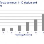
It lays the foundation for the Stochastics Resolution Gap
Chris Mack, the CTO of Fractilia, recently wrote of the “Stochastics Resolution Gap,” which is effectively limiting the manufacturability of EUV despite its ability to reach resolution limits approaching 10 nm in the lab [1,2]. As researchers have inevitably found, … Read More
-We attended the SPIE lithography Conference in San Jose
-No significant news or announcements on EUV
-Focus on 500WPM target and High & Hyper NA rollout
-AMAT overblown Sculpta-Not exactly what its cracked up to be
We have been attending SPIE for many years now and are happy to see a return to pre Covid levels… Read More
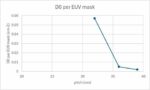
At this year’s SPIE Advanced Lithography conference, changes to EUV masks were particularly highlighted, as a better understanding of their behavior is becoming clear. It’s now confirmed that a seemingly symmetric EUV mask absorber pattern does not produce a symmetric image at the wafer, as a conventional DUV … Read More
-KLA has another great QTR in face of overwhelming demand
-Supply chain issues obliterated by backlog
-Longer term technology leadership concerns are increasing
-We see limited upside near term & remain cyclically cautious
Another great quarter- demand remains super strong
KLA’s performance remains great as does… Read More
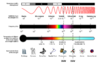
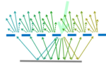
As feature sizes have shrunk, the semiconductor industry has moved from simple, single-exposure lithography solutions to increasingly complex resolution-enhancement techniques and multi-patterning. Where the design on a mask once matched the image that would be produced on the wafer, today the mask and resulting image … Read More
The annual SPIE Advanced Lithography Conference kicked off last night with vendor sponsored networking events and such. SPIE is the international society for optics and photonics but this year SPIE Advanced Lithography is all about the highly anticipated EUV technology. Scotten Jones and I are at SPIE so expect more detailed… Read More
As I write about integrated photonics I continue to hear from long-time experts in the field who lament that integrated photonics has been around for decades and other than telecom/datacom, it seems to never be a mainstream technology. It’s hard to argue that this time around it will be different as those people have lived through… Read More
For me personally EUV has been something of a roller coaster ride over the last several years. I started out a strong believer in EUV but then at the SPIE Advanced Lithography Conference in 2014 TSMC gave a very negative assessment of EUV, and there was a SEMATECH paper on high NA EUV that struck me as extremely unlikely to succeed. I … Read More