Having the right tool for the job at hand is always a joy, and when your IC project involves RTL code, gates, transistors and even parasitic interconnect, then you need some EDA tool help for debugging and finding out why your design behaves the way it is. An FAE named Sujit Roy did a conference call with me last week to show what StarVision… Read More
Tag: spef
Webinar: Designing Complex SoCs and Dealing with Multiple File Formats
In SoC design it’s all about managing complexity through modeling, and the models that make up IC designs come in a wide range of file formats like:
- Transistor-level , SPICE
- Interconnect parasitics, SPEF
- Gate and RTL, Verilog, VHDL
Even with standard file formats, designers still have to traverse the hierarchy to find out… Read More
Challenges in IP Qualification with Rising Physical Data
With every new technology node, there are newer physical effects that need to be taken into account. And every new physical effect brings with itself several new formats to model them. Often a format is also associated with several of its derivatives, sometimes an standard reincarnation of a proprietary format further evolved… Read More
Complete SoC Debugging & Integration in a Single Cockpit
These days it’s common to expect large digital designs, analog blocks, custom IPs, glue logic, interfaces and interconnects all developed separately, perhaps by different vendors / teams, but integrated together in a single environment forming an SoC. The SoC can have multiple clock domains and can work in multiple modes of … Read More
Expert Tool to View and Debug Design Issues at Spice Level
Spice view of a design, block or fragment of the design is probably the lowest level of functional description of a circuit in terms of transistors, resistors, capacitors, interconnect and so on, which in several ways acts as an ultimate proof of pudding for any semiconductor design before manufacturing. However, it’s generally… Read More
Concept Engineering Showcases Effective SoC Debugging Techniques
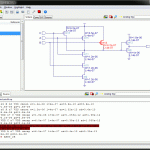
In a complex environment of semiconductor design where an SoC can have several millions of gates and multiple number of IPs at different levels of abstractions from different sources integrated together, it becomes really difficult to understand and debug the overall SoC design. Of course, along with the SoC integration, optimization… Read More
FinFET & Multi-patterning Need Special P&R Handling
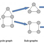
I think by now a lot has been said about the necessity of multi-patterning at advanced technology nodes with extremely low feature size such as 20nm, because lithography using 193nm wavelength of light makes printing and manufacturing of semiconductor design very difficult. The multi-patterning is a novel semiconductor manufacturing… Read More
Mixed-Signal SoC Debugging & IP Integration Made Easy
A semiconductor SoC design can have multiple components at different levels of abstractions from different sources and in different languages. While designing an SoC, IPs at different levels have to be integrated without losing the overall design goals. Of course, quality of an IP inside and outside of an SoC must be tested thoroughly.… Read More
What Makes A Designer’s Day? A Bottleneck Solved!
In an environment of SoCs with tough targets of multiple functionalities, smallest size, lowest power and fastest performance to achieve within a limited design cycle window in order to meet the rigid time-to-market requirements, any day spent without success becomes very frustrating for a designer. Especially during tape-out… Read More
ST Endorses PowerArtist with ARM Cores & FDSOI libs
It was an interesting webinar I attended, presented by STMicroelectronicson how they are benefited in power saving and thermal dissipation by using FDSOI technology and also by using PowerArtist in their design. So, it’s an advantage from both sides – semiconductor technology and semiconductor design tool. It’s worth attending… Read More


