You are currently viewing SemiWiki as a guest which gives you limited access to the site. To view blog comments and experience other SemiWiki features you must be a registered member. Registration is fast, simple, and absolutely free so please,
join our community today!
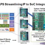
SoC’s are now dominated by IP blocks sourced either from 3rd parties or internal design teams. This means that IP is now critical to the success of the SoC, yet it is part of the design that teams have the least control over, or visibility into. Most design teams utilize at best ad-hoc methods to manage this IP, and the few that utilize… Read More
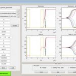
Metastability is a critical SoC failure mode that occurs at the interface between clocked and clockless systems. It’s a risk that must be carefully managed as the industry moves to increasingly dense designs at 28nm and below. Blendics is an emerging technology company that I have been working with recently, their MetaACE… Read More
IR drop analysis across your board, package and SoC ensures that your Power Delivery Network (PDN) is robust, and that your system will function to spec. There are both static and dynamic approaches to IR drop analysis of a full-chip with billions of transistors, while the dynamic approach produces the most accurate results compared… Read More
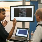
At DAC you can measure buzz by how many people are crowded into your booth. I saw a crowd at the Oasys booth, so stopped to take in their 10 minute overview presentation. Here’s what I learned.… Read More
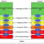
Interface IP typically consists of multiple layers, most importantly a PHY (level 1) analog (or mixed signal) block that handles the interface to the outside world and a number of levels of digital controllers. The interfaces between all these levels, especially between the PHY and the controller, is often defined by the interface… Read More
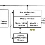
My last chip design at Intel was a GPU called the 82786and the architects of the chip wrote a virtual prototype using the MAINSAIL language. By using a virtual prototype they were able to:
- Simulate bus traffic, video display and video RAM
- Determine throughput
- Measure latency
- Verify that bus priorities were working
- Optimize the
…
Read More
We’ve been talking about the different technologies for FPGA-based SoC prototyping a lot here in SemiWiki. On the surface, the recent stories all start off pretty much the same: big box, Xilinx Virtex-7, wanna go fast and see more of what’s going on in the design. This is not another one of those stories. I recently sat down with Mick… Read More
Last month at DAC I learned how IBM, Cadence, ARM, GLOBALFOUNDRIES and Samsung approach the challenges of SoC design, EDA design and fabrication at the 20nm node. Today I followed up by reading a white paper on 20nm IC design challenges authored by Cadence, a welcome relief to the previous marketing mantra of EDA 360.
Here’s… Read More