You are currently viewing SemiWiki as a guest which gives you limited access to the site. To view blog comments and experience other SemiWiki features you must be a registered member. Registration is fast, simple, and absolutely free so please,
join our community today!
In today’s rapidly evolving semiconductor industry, the design and integration of intellectual property (IP) play a pivotal role in achieving competitive advantage and market success. Whether sourced from commercial IP providers or developed in-house, ensuring that IP designs are compliant with signoff requirements… Read More
Over the last few years, there has been an increase in news about quantum computing. Much of this news coverage has been around computing supremacy, potential threats to information security and quantum cryptography. While the field of quantum computing is still in its early stages, there are several companies who have already… Read More
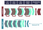
The evolution of space-based applications continues to drive innovation across government and private entities. The new demands for advanced capabilities and feature sets have a direct impact on the underlying hardware, driving companies to migrate to smaller geometries to deliver the required performance, area, and power… Read More
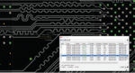
Printed Circuit Boards (PCBs) are the foundation of modern electronics, and designing them efficiently is complex. Design automation and advanced PCB routing have transformed the process, making it faster and more reliable. Design automation streamlines tasks, reduces errors, and ensures consistency. Advanced PCB routing… Read More
Jean-Marie Brunet is Vice President and General Manager of Siemens Hardware-Assisted Verification. He and I spoke recently about how different his hardware group is from the rest of the software-centric EDA product space and why a hardware-oriented EDA vendor like Siemens fully understands the challenges of the chip design… Read More
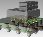
While the leap from traditional SoC/IC designs to Three-Dimensional Integrated Circuits (3DICs) designs brings new benefits and opportunities, it also introduces new challenges. The benefits include performance, power efficiency, footprint reduction and cost savings. The challenges span design, verification, thermal… Read More
One of the most promising advancements in the semiconductor field is the development of 3D Integrated Circuits (3D ICs). 3D ICs enable companies to partition semiconductor designs and seamlessly integrate silicon Intellectual Property (IP) at the most suitable process nodes and processes. This strategic partitioning yields… Read More
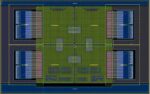
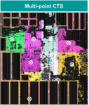
If you have anything to do with the semiconductor industry, you already know that one of the hottest areas for both manufacturing and EDA are systems designed with advanced packaging, basically putting more than one die (aka chiplets) in the same package.
When 3D packaging was first introduced, there were not really any effective… Read More
You are probably familiar with the acronym PPA, which stands for Power/Performance/Area. Sometimes it is PPAC, where C is for cost, since there is more to cost than just area. For example, did you know that adding an additional metal layer to a chip dramatically increases the cost, sometimes by millions of dollars? It requires a … Read More
Advanced process nodes create challenges for EDA both in handling ever larger designs and increasing design process complexity.
Shift-left design methodologies for design cycle time compression are one response to this. And this has also forced some rethinking about how to build and optimize design tools and flows.
SemiWiki… Read More