You are currently viewing SemiWiki as a guest which gives you limited access to the site. To view blog comments and experience other SemiWiki features you must be a registered member. Registration is fast, simple, and absolutely free so please,
join our community today!
By Shehab Ashraf
As semiconductor technology scales and device complexity increases, accurately modeling the parasitic effects of metal fill has become critical for circuit performance, power integrity, and reliability. Metal fill is a crucial part of the manufacturing process, ensuring uniform layer density, improving… Read More
Now that the dust has settled, I will give you my take on the Intel Foundry event. Some might call me a semiconductor event critic as I have attended hundreds of them over the last 40 years starting with the Design Automation Conference in 1984. Foundry events are my favorite because they really are the pulse of the semiconductor industry,… Read More
We started working with Alphawave at the end of 2020 with a CEO Interview. I had met Tony Pialis before and found him to be a brilliant and charismatic leader so I knew it would be a great collaboration. Tony was already an IP legend after his company was acquired by Intel. After 4+ years at Intel Tony co-founded Alphawave in 2017. Today,… Read More
In today’s digital landscape, data security has become an indispensable feature for any data transfer protocol, including Peripheral Component Interconnect Express (PCIe). With the rising frequency and sophistication of digital attacks, ensuring data integrity, confidentiality, and authenticity during PCIe transport… Read More
I’ve known about DRC (Design Rule Checking) for IC design, and the same approach can also be applied to PCB design. The continuous evolution of electronics has led to increasingly intricate PCB designs that require Electrical Rule Checking (ERC) to ensure that performance goals are met. This complexity poses several challenges… Read More
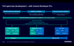
At the heart of the shift-left strategy is the goal of moving traditionally late-stage tasks—such as software development, validation, and optimization—earlier in the design process. This proactive approach allows teams to identify and resolve issues before they escalate, reducing costly rework and shortening the overall… Read More
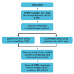
Improve productivity by shifting left LVS
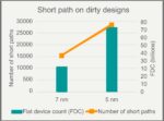
In modern semiconductor design, technology nodes continue to shrink and the complexity and size of circuits increase, making layout versus schematic (LVS) verification more challenging. One of the most critical errors designers encounter during LVS runs are shorted nets. Identifying… Read More
Functional coverage acts as a guide to direct verification resources by identifying the tested and untested portions of a design. Functional coverage is a user-defined metric that assesses the extent to which the design specification, as listed by the test plan’s features, has been used. It can be used to estimate the presence… Read More
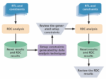
The complexity of System-on-Chip (SoC) designs continues to rise at an accelerated rate, with design complexity doubling approximately every two years. This increasing complexity makes verification a more difficult and time-consuming task for design engineers. Among the key verification challenges is managing reset domain… Read More
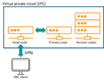
Embracing cloud computing is highly attractive for users of electronic design automation (EDA) tools and flows because of the productivity gains and time to market advantages that it can offer. For Siemens EDA customers engaged in designing large, cutting-edge chips at advanced nanometer scales, running Calibre® design stage… Read More