You are currently viewing SemiWiki as a guest which gives you limited access to the site. To view blog comments and experience other SemiWiki features you must be a registered member. Registration is fast, simple, and absolutely free so please,
join our community today!
The big challenge with audio is that there are so many standards. Some of this is for historical reasons since audio for mobile (such as mp3), for the home (Dolby 5.1) and for cell-phone voice encoding/decoding have all had very different requirements, different standard setters and so on. But gradually everything is coming together.… Read More
Just how many hands have touched your SoC design by the time it goes to manufacturing? Clearly the more hands that touch it, the more complex the design is, making it more difficult to meet your product requirements. The commercial semiconductor IP dilemma is that not only are you using the same IP as your competitors, you are exponentially… Read More
Joe Sawicki is the VP and General Manager at Mentor Graphics for the Design-to-Silicon Division where the Calibre product line is developed. We met today in Wilsonville, Oregon to review the challenges in IC design, processing and manufacturing.… Read More
T’is the season to be jolly…and to predict the next year’s semiconductor market.
KPMG does a regular survey of senior executives in semiconductor companies to get their outlook on the year ahead. The message this year is mixed. 41% of executives expected their business to grow by more than 5% next year, which sounds not too bad until… Read More
Immediately following Intel’s announcement that they expected Q4 revenue to come up short by $1B, Rory Read the new CEO of AMD, countered that they were on track to meet their original guidance (see article). Furthermore, “In 1Q and 2Q, maybe you see some manifestations, but I wouldn’t bet against the supply chain,”… Read More
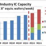
SICAS (Semiconductor Industry Capacity Statistics) has released its 3Q 2011 data, available through the SIA at: SICAS data . Beginning with 2Q 2011 the SICAS membership list no longer includes the Taiwanese companies Nanya Technology, Taiwan Semiconductor Manufacturing Company Ltd. (TSMC) or United Microelectronics Corporation… Read More
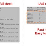
LVS Challenges at Advanced Nodes
Accurate, comprehensive device recognition, connectivity extraction, netlist generation and, ultimately, circuit comparison becomes more complex with each new process generation. As the number of layers and layer derivations increases the complexity of devices, especially Layout Dependent… Read More
Conspiracy theories abound! The inside story of the Synopsys (SNPS) acquisition of Magma (LAVA) brings us back to the 1990’s tech boom with shady investment bankers and pump/dump schemes. After scanning my memory banks and digging around Silicon Valley for skeletons with a backhoe here is what I found out:
The Commission… Read More
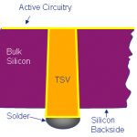
3D IC design and what has come to be known as 2½D IC design, with active die on a silicon interposer, require new approaches to verification since the through silicon vias (TSVs) and the fact that several different semiconductor processes may be involved create a new set of design challenges
The power delivery network is a challenge… Read More
Low power techniquesby Paul McLellan on 12-08-2011 at 5:49 pmCategories: General
There was recently a forum discussion about the best low power techniques. Not surprisingly we didn’t come up with a new technique nobody had ever thought of but it was an interesting discussion.
First there are the techniques that by now have become standard. If anyone wants more details on these then two good resources are… Read More