You are currently viewing SemiWiki as a guest which gives you limited access to the site. To view blog comments and experience other SemiWiki features you must be a registered member. Registration is fast, simple, and absolutely free so please,
join our community today!
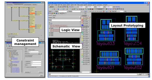
Over the years many attempts have been made to increase the level of automation in analog design. Most of these have not been especially successful. Probably part of the reason was inadequate technology but also there is an attitude that “real” analog designers design polygons on the bare silicon. I think two things… Read More
EUV is the great hope for avoiding having to go to triple (and more) patterning if we have to stick with 193nm light. There were several presentations at Semicon about the status of EUV. Here I’ll discuss the issues with EUV lithography and in a separate post discuss the issues about making masks for EUV.
It is probably worth … Read More
I attended a panel session followed by a party during Semicon to celebrate Soitec’s 20th birthday. Officially it was titled An Insider’s Look at the Future of Mobile Technologies. But in reality it was a look at the future possibilities for SOI.
Silicon on Insulator (SOI) has been a sort of bastard child of semiconductor.… Read More
One of the presenters at the standing-room only litho session at Semicon this week was Serge Tedesco, the litho program manager at CEA-Leti in Grenoble France. He is running a program called IMAGINE for maskless lithography. Chips today are built using a reticle (containing the pattern for that layer of the chip) which is exposed… Read More
There is an interesting Gizmodo review of an HTC Android-based smartphone. The basically positive review (as good as the iPhone, best Android phone at the time) ends up with an update:UPDATE: After more extensive testing there’s something a little weird going on. You’ll probably only see this while gaming, but there’s… Read More
Whenever I write about the handset industry, lots of people seem to be interested. As I’ve said before, my go to person for the industry but especially for Nokia, is Tomi Ahonen. He has written a long (and I mean long, it is nearly 30,000 words) indictment of Elop’s tenure at Nokia and how he has destroyed one of the most … Read More
I have been spending some time at Semicon West at the Moscone center the last couple of days. Since it was only a month ago that I was there for DAC, the first contrast is the size of the show. DAC didn’t fill Moscone South. Semicon fills Moscone South, and North, and the corridor between. And Moscone West on the other side of 4th … Read More
The 1st Atrenta Technology Forum in Japan (well, it used to be the user group meeting, so it’s only the first in a very technical sense) is next week on July 19th from 1pm until 5.15pm. It will be held in the Shin-Yokohama Kokusai Hotel (how to access it here).
In the unlikely event that non-Japanese are reading this blog, here’s… Read More
As 2D device scaling becomes impractical, 3D-IC integration is emerging as the natural evolution of semiconductor technology; it is the convergence of performance, power and functionality. Some of the benefits of 3D-IC, such as increasing complexity, improved performance, reducing power consumption and decreasing footprints,… Read More
If you are in Asia then the Synopsys user group SNUG is coming up, soon in Japan and next month in China. Actually if you are in India I’m afraid you already missed it last month, just after DAC.
SNUG Japan is on 12th July in a couple of days time from 10am until 8pm in Tokyo.
In China there are 3 between August 14th and 21st
…
Read More