You are currently viewing SemiWiki as a guest which gives you limited access to the site. To view blog comments and experience other SemiWiki features you must be a registered member. Registration is fast, simple, and absolutely free so please,
join our community today!
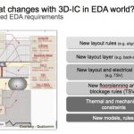
A couple of weeks ago was the 3D Architectures for Semiconductor Integration and Packagingconference in Redwood City. Cadence presented the changes that they have been making to their tool flow to enabled 2.5D (interposer-based) and true 3D TSV-based designs. You know what TSV stands for by now right? Through-silicon-via, … Read More
Shipments of semiconductor manufacturing equipment have been trending downward since June 2012, based on combined data from SEMI for North American and European manufacturers and from SEAJ for Japanese manufacturers. The market bounced back strongly in late 2009 and in 2010 after the 2008 downturn to return to the $3 billion… Read More
There are two primary microprocessor companies in the world these days: Intel and ARM. Of course there are many others but Intel is dominant on the PC desktop (including Macs) and ARM is dominant in mobile (including tablets).
One of the keynotes at last month’s Jasper User Group (JUG, not the greatest of acronyms) was by Bob… Read More
Design For Manufacturing (DFM) is the art and science of making an IC design yield better in order to receive a higher ROI. Ian Smith, an AE from Mentor in the Calibre group presented a pertinent webinar, IP Scoring Using TSMC DFM Kits. I’ll provide an overview of what I learned at this webinar.… Read More
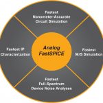
Analog, mixed-signal, RF, and custom digital circuitry implemented in GHz nanometer CMOS introduce a new class of design and verification challenges that traditional transistor‑level simulators cannot adequately address. Berkeley Design Automation, Inc., (BDA) was founded in 2003 by Amit Mehrotra and Amit Narayan,… Read More
Double patterning at 20nm is one of those big unavoidable changes that it is almost impossible to know too much about. Mentor’s David Abercrombie, DFM Program Manager for Calibre, has written a series of articles detailing the multifaceted impacts of double patterning on advanced node design and verification. There is… Read More
Late in January it is DesignCon at the Santa Clara convention center from January 28th-31st. Details are here.
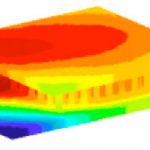
On Tuesday from 11.05 to 11.45 Apache and Ansys will be presenting on Thermal Co-analysis of 3D IC/packages/system. This is being presented by a whole team of people: Stephen Pan, senior product specialist at ANSYS; Norman… Read More
The 26th Conference on VLSI Design will be in Pune, India from January 5th to 10th at the Hyatt Regency. Details on the conference here. Registration here. I happened to be involved in the first of these conferences, which was held in Edinburgh where I was wrapping up my PhD. It was in the considerably less palatial surroundings of … Read More
One of the largest software companies in the world, Synopsys is a market and technology leader in the development and sale of electronic design automation (EDA) tools and semiconductor intellectual property (IP). Synopsys is also a strong supporter of local education through the Synopsys Outreach Foundation. Each year in multiple… Read More
Happy Holidaysby Paul McLellan on 12-10-2012 at 3:00 pmCategories: EDA
At times of this year, companies usually get their salespeople to submit the names and addresses of all their customers. They then get an expensive card printed and mail it out. What the recipient does is anyone’s guess, from throwing it straight in the bin to using it to decorate the office.
Atrenta decided to do something … Read More