You are currently viewing SemiWiki as a guest which gives you limited access to the site. To view blog comments and experience other SemiWiki features you must be a registered member. Registration is fast, simple, and absolutely free so please,
join our community today!
Last week I met with Joseph Davis, Ph.D. at Mentor Graphics in Wilsonville, Oregon to learn about a new product designed for full-custom IC layout designers to improve productivity.
The traditional flow for full-custom IC layout designers has been nearly unchanged for decades:
- Read a schematic or use Schematic Driven Layout
…
Read More
This is just another blog about Carl Icahn and his quest to conquer EDA, when in fact EDA is conquering him. It includes highlights from my dinner with Mentor Graphics and Physicist Brian Greene, the Mentor Q4 conference call, and meeting Mentor CEO Wally Rhines at DvCon 2011.
It wasn’t just the free food this time, dinner with Brian… Read More
Abstract:
There has been a remarkable acceleration in the adoption of advanced verification methodologies, languages and new standards. This is true across all types of IC design and geographic regions. Designers and verification engineers are surprisingly open to new approaches to keep pace with the relentless rise in design… Read More
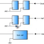
Multiple, independent clocks are quintessential in SoCs and other complex ASICs today. In some cases, such as in large communications processors, clock domains may number in the hundreds. Clock domain crossings pose a growing challenge to chip designers, and constitute a major source of design errors–errors that can… Read More
A growing number of reports highlight a class of design errors that is difficult to check using more traditional methods, and can potentially affect a wide range of IC designs, especially where high reliability is a must.By Matthew Hogan
Today’s IC designs are complex. They contain vast arrays of features and functionality in … Read More
During the most recent conference call (transcript), TSMC not only beat revised estimates and announced record spending levels for 2011, Morris Chang also officially announced that a 450mm fab (Fab 12 Phase VI) is currently in the planning stages with target production @ 20nm in 2015. This is HUGE!
According to Morris Chang:
“For… Read More
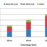
Last week I talked with two experts at Mentor about the challenges of getting IC designs into the 32nm/28nm node on the Common Platform (IBM, GLOBALFOUNDRIES and Samsung). Global Foundries issued a press release talking about how the four major EDA companies have worked together to qualify EDA tools for this node.
Sudhakar Jilla,… Read More
Is EDA still an appropriate term for what we do? What applications will drive future semiconductor design innovation? Will further consolidation be required for EDA to thrive again? They are all good questions, questions that will hopefully be properly addressed at the EDAC CEO Forecast and Industry Vision event next week but… Read More
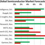
Of course these are rolling forecasts which means they change every month, until they get them right. The missing forecaster here is Mike Cowen, developer of the Cowan LRA Model which forecasts global semiconductor sales. Mike has 2011 at a hilarious 2.3%! Below are the mid year market forecasts which were revised significantly… Read More
More consolidation is coming to EDA and so is the Federal Trade Commission. Corporate raider Carl Ichan owns 15% of Mentor Graphics and now owns 1% of Cadence. Ichan buddy multi billionaire George Soros, a long time CDNS investor, just purchased more than 76 million convertible notes of MENT.You do the math…
Unfortunately the FTC… Read More