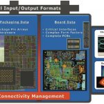
A new term has entered the vernacular of electronic design engineering — pathfinding. The complexity of the functionality to be integrated and the myriad of chip, package, and board technologies available make the implementation decision a daunting task. Pathfinding refers to the method by which the design space of technology… Read More
Tag: semiconductor manufacturing
The Death of Moore’s Law
For the last several years, people have predicted the end of Moore’s Law. The reasoning is that there is a limit at which one can’t shrink transistors any further. A reoccurring comment has been “You can’t divide an atom.” I had assumed that its demise would be at the hands of a new paradigm like quantum computing. Now, with Intel’s … Read More
IEDM 2015 Blogs – Part 1 – Overview
The International Electron Devices Meeting (IEDM) is one of, if not the premier conference for semiconductor process technology. The 2015 meeting just finished up on Wednesday, December 9th.
This year’s meeting was held from Saturday, December 5[SUP]th[/SUP] through Wednesday, December 9[SUP]th[/SUP] in Washington DC.… Read More
Moore’s law limitations and gravitational collapse at lower process nodes
As stated in my previous article, about the complexity of the SOC with billions of transistors. It is essential to consider the real practical scenario for the two dimensional verses three dimensional structure of the chip. Although the new technological changes and evolution for the shrinking process node can create ease for… Read More
M&A Frenzy in the Chip Industry, the Growth of GaN, and Why It Matters
If expanding industries typically indicate vibrancy, a race to acquire and consolidate is generally reflective of the opposite – a period of slowed growth in mature, once high-flying categories. And while many industries experience a period of stardom, followed by a sharp and steady decline, we should be extremely worried when… Read More
Extending EUV Lithography
I have previously written about SPIE day 1 and 2 so I want to wrap up my coverage with some impressions from days 3 and 4. My single biggest take away from the conference is that EUV has made tremendous progress in the last 12 months. Last year the mood of the conference was in my opinion pessimistic with respect to EUV, this year the mood… Read More
Samsung Foundry Debuts 10nm Wafer!
The Samsung Smart, Connected Lifestyle event was last night at the Bently Reserve in San Francisco. Getting into San Francisco was no picnic with all of the roadwork and new building construction. We even saw people drive up on the sidewalk to get around car clogs. It really was crazy but definitely worth it after seeing the first … Read More
ASMC 2015 Preview
From May 3[SUP]rd[/SUP] to May 6[SUP]th[/SUP] the 26[SUP]th[/SUP] annual Advanced Semiconductor Manufacturing Conference (ASMC) will be held in Saratoga Springs, New York.
The ASMC offers a unique view of challenges to the semiconductor industry focusing on things like defect reduction, metrology and fab operations. In… Read More
Semiconductor CAPEX Growth Increases Fab Equipment Spending!
With worldwide capex growth of 8%, fab equipment spending is expected to increase by 15% in 2015, according to the most recent edition of the SEMI (www.semi.org) World Fab Forecast. SEMI’s data also predicts a slowdown of fab equipment spending in 2016 to low single … Read More


