Earlier this month, TechInsights did a teardown of the Kirin 9030 chip found in Huawei’s Mate 80 Pro Max [1]. Two clear statements were made on the findings: (1) the transistor density of SMIC’s “N+3” process was definitely below that of the earlier 5nm processes from Samsung and TSMC, and (2) metal pitch was aggressively scaled
Tag: saqp
Huawei’s and SMIC’s Requirement for 5nm Production: Improving Multipatterning Productivity
There has been much interest in Huawei’s and SMIC’s plans for 5nm production in the near future. Since there is no use of EUV in China, immersion DUV lithography (with a 76 nm pitch resolution) is expected to be used along with pitch quartering to achieve pitches in the 20-30 nm range expected for the 5nm and 3nm nodes [1].… Read More
Etch Pitch Doubling Requirement for Cut-Friendly Track Metal Layouts: Escaping Lithography Wavelength Dependence
The 5nm foundry node saw the arrival of 6-track standard cells with four narrow routing tracks between wide power/ground rails (Figure 1a), with minimum pitches of around 30 nm [1]. The routing tracks require cuts [2] with widths comparable to the minimum half-pitch, to enable the via connections to the next metal layer with the… Read More
The Complexities of the Resolution Limits of Advanced Lithography
For advanced lithography used to shrink semiconductor device features according to Moore’s Law, resolution limits are an obvious consideration. It is often perceived that the resolution limit is simply derived from a well-defined equation, but nothing can be further from the truth.
Optical Lithography: the fine print
… Read MoreCD-Pitch Combinations Disfavored by EUV Stochastics
Ongoing investigations of EUV stochastics [1-3] have allowed us to map combinations of critical dimension (CD) and pitch which are expected to pose a severe risk of stochastic defects impacting the use of EUV lithography. Figure 1 shows a typical set of contours of fixed PNOK (i.e., the probability of a feature being Not OK due… Read More
Toshiba Cost Model for 3D NAND
Toshiba (now known as Kioxia) was the first company to propose a 3D stacked version of NAND Flash memory called BICS [1]. BICS (BIt Cost Scalable) Flash used explicit process cost reduction based on depositing and etching multiple layers at once, avoiding multiple lithography steps. This strategy replaced the usual approach… Read More
Fully Self-Aligned 6-Track and 7-Track Cell Process Integration
For the 10nm – 5nm nodes, the leading-edge foundries are designing cells which utilize 6 or 7 metal tracks, entailing a wide metal line for every 4 or 5 minimum width lines, respectively (Figure 1).
Figure 1. Left: a 7-track cell. Right: a 6-track cell.
This is a fundamental vulnerability for lithography, as defocus can change… Read More
Application-Specific Lithography: a 28 nm Pitch DRAM Active Area
In the recent DRAM jargon, “1X”, “1Y”, “1Z”, etc. have been used to express all the sub-20 nm process generations. It is almost possible now to match them to real numbers which are roughly the half-pitch of the DRAM active area, such as 1X=18, 1Y ~ 17, etc. At this rate, 14 nm is somewhere around
Application-Specific Lithography: The 5nm 6-Track Cell
An update is now available here: Application-Specific Lithography: Patterning 5nm 5.5-Track Metal by DUV
The 5nm foundry (e.g., TSMC) node may see the introduction of 6-track cells (two double-width rails plus four minimum-width dense lines) with a minimum metal pitch in the neighborhood of 30 nm. IMEC had studied a representative… Read More
Feature-Selective Etching in SAQP for Sub-20 nm Patterning
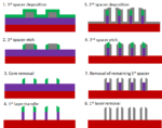
Self-aligned quadruple patterning (SAQP) is the most widely available technology used for patterning feature pitches less than 38 nm, with a projected capability to reach 19 nm pitch. It is actually an integration of multiple process steps, already being used to pattern the fins of FinFETs [1] and 1X DRAM [2]. These steps, shown… Read More


