In today’s rapidly evolving semiconductor industry, the design and integration of intellectual property (IP) play a pivotal role in achieving competitive advantage and market success. Whether sourced from commercial IP providers or developed in-house, ensuring that IP designs are compliant with signoff requirements… Read More
Tag: physical verification
Optimizing Shift-Left Physical Verification Flows with Calibre
Advanced process nodes create challenges for EDA both in handling ever larger designs and increasing design process complexity.
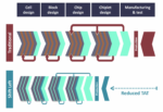
Shift-left design methodologies for design cycle time compression are one response to this. And this has also forced some rethinking about how to build and optimize design tools and flows.
SemiWiki… Read More
Physical Verification with IC Validator
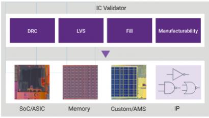
If a picture worths a thousand words, a tapeout quality SoC design with billions of polygons would compose a good book. To proofread this final design transformation format requires a foundry driven DRC/LVS signoff solution that nowadays is becoming more complex with further process scaling and shrinking pitch dimension.
Despite… Read More
High Calibre Development Keeps Mentor on Top of the Game
One might be tempted to think that technology driven gains in computer performance might be enough to keep up with the needs of design and verification tools. We know that design complexity is increasing at a rate predicted by Moore’s Law. We also know that the performance of the computers used during IC development benefit from … Read More
Show Me How To Get Better DRC and LVS Results For My SoC Design
Most IC engineers learn best by hands-on experience when another more experienced person can show us what to do. If you cannot find that experienced person, then the next best thing is a video from an expert. I was surprised to find out that video was so important today that the #2 most viewed web site on the Internet was www.youtube.com… Read More
Going up…3D IC design tools
3D and 2.5D (silicon interposer) designs create new challenges for EDA. Not all of them are in the most obvious areas. Mentor has an interesting presentation on what is required for verification and testing of these types of designs. Obviously it is somewhat Mentor-centric but in laying out the challenges it is pretty much agnostic.… Read More
Speeding SoC timing closure
As chips have become larger, one of the more challenging steps is full-chip signoff. Lots of other steps in the design process can work on just a part of the problem, but by definition full-chip signoff has to work on the full chip. But it is not just that chips have got larger, the number of corners that need to be validated has also exploded.… Read More


