You are currently viewing SemiWiki as a guest which gives you limited access to the site. To view blog comments and experience other SemiWiki features you must be a registered member. Registration is fast, simple, and absolutely free so please,
join our community today!
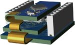
From Zion Research I learned that the flexible electronics market was about $13.2B in 2021 and growing at a CAGR of 21%, so that was impressive. There are several factors that make rigid-flex circuit so attractive, like: space efficiency, reduced weight, enhanced reliability, improved signal integrity, streamlined assembly,… Read More
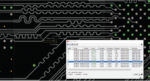
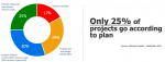
PCB designers can perform pre-route simulations, follow layout and routing rules, hope for the best from their prototype fab, and yet design errors cause respins which delays the project schedule. Just because post-route analysis is time consuming doesn’t mean that it should be avoided. Serial links are found in many PCB designs,… Read More
I knew that HDMI was a popular standard used to connect consumer products like a monitor to a laptop, but most professional video and broadcast systems use the SDI (Serial Digital Interface) connector standard. Pleora Technologies, founded in 2000, currently serves the machine vision and manufacturing markets, including those… Read More
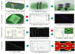
Printed Circuit Boards (PCBs) are the foundation of modern electronics, and designing them efficiently is complex. Design automation and advanced PCB routing have transformed the process, making it faster and more reliable. Design automation streamlines tasks, reduces errors, and ensures consistency. Advanced PCB routing… Read More
Generative AI is all the rage with systems like ChatGPT, Google Bard and DALL-E being introduced with great fanfare in the past year. The EDA industry has also been keen to adopt the trends of using AI techniques to assist IC engineers across many disciplines. Saugat Sen, Product Marketing at Cadence did a video call with me to explain… Read More
This. AI in PCB design is not a new idea. Other PCB software companies also make that claim. But when a mainstream systems technology company like Siemens talks about the subject, that is noteworthy. They already have an adaptive user interface (UI) for their mechanical modeling suite and to assist in low-code development for application… Read More
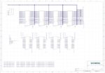
My IC design career started just a few years before PADS got started in 1985 with a DOS-based tool for PCB design. A lot has changed since then, as PADS was acquired by Mentor Graphics in 2001, and continued to grow under Siemens EDA, now with four versions to choose from, where the top version is called PADS Professional Premium:
…
Read More
I can remember back in the 1980s how Apollo workstations were quite popular, because they accelerated the graphics display time for EDA tools much better than competitive hardware. Fast forward to 2022 and we have the same promise of speeding up EDA tools like PCB layout editing by using a GPU. At the 58th DAC there was a session called,… Read More
The last session I attended at DesignCon 2020 wasn’t a session at all. Rather it was an interactive discussion with Todd Westerhoff, product manager for electronic board systems at Mentor Graphics. Todd made some observations about the way high-performance PCBs are designed today and perhaps the way they should be designed. … Read More
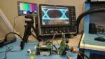
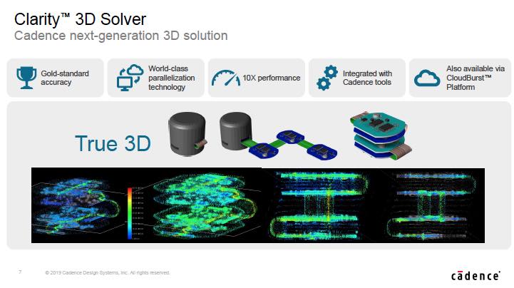
The need for full wave EM solvers has been creeping into digital design for some time. Higher operating frequencies – like those found in 112G links, lower noise margins – caused by multi level signaling such as in PAM-4, and increasing design complexity – as seen in RDL structures, interposers, advanced connector… Read More