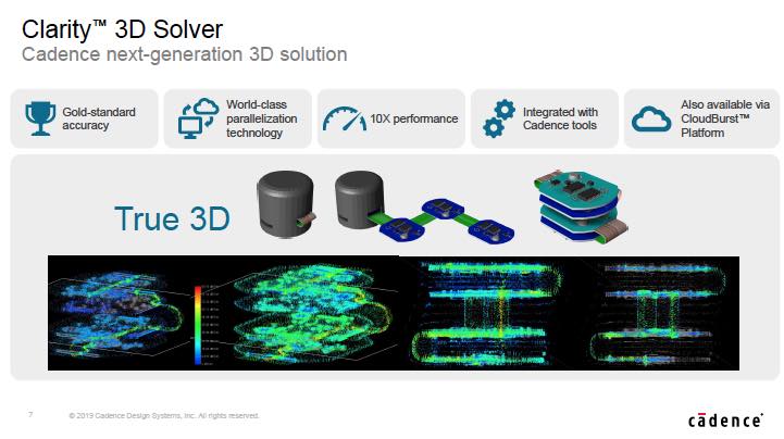
Signal Integrity (SI) and Power Integrity (PI) issues are critical to analyze, ensuring the proper operation of PCB systems and IC packages, yet the computational demands from EDA tools can cause engineers to only analyze what they deem are critical signals, instead of the entire system. Cadence has managed to overcome this SI/PI… Read More
Tag: package
Maximizing ASIC Performance through Post-GDSII Backend Services
ASICs by definition are designed to meet the respective applications’ requirements. ASIC engineers deploy various design techniques to maximize performance, minimize power and reduce chip size. But is there more that can be done after the GDSII is taped out? A recent press release from Alchip Technology dated Feb 4, 2021 claims… Read More
Optimizing High Performance Packages calls for Multidisciplinary 3D Modeling
For all the time we spend thinking and talking about silicon design, it’s easy to forget just how important package design is. Semiconductor packages have evolved over the years from very basic containers for ICs into very specialized and highly engineered elements of finished electronic systems. They play an important role … Read More
Solving the EM Solver Problem
The need for full wave EM solvers has been creeping into digital design for some time. Higher operating frequencies – like those found in 112G links, lower noise margins – caused by multi level signaling such as in PAM-4, and increasing design complexity – as seen in RDL structures, interposers, advanced connector… Read More
At Last, Package and Chip integration for RF Design
It seems that it has always been that there were packages and ICs, and in the design tool world “never the twain shall meet”. The tools for designing packages were completely separate from the tools used to design IC’s. This was so profoundly true that even after Cadence merged with Valid Logic back in the early 90’s, their Allegro … Read More
Solving and Simulating in the New Virtuoso RF Solution
Cadence has done a good job of keeping up with the needs of analog RF designs. Of course, the term RF used to be reserved for a thin slice of designs that were used specifically in RF applications. Now, it covers things like SerDes for networking chips that have to operate in the gigahertz range. Add that to the trend of combining RF and… Read More
Power Noise Sign-off at #53DAC
When I hear the company name of ANSYS the first EDA tool category that comes to mind is power noise sign-off. Going to DAC is a great way to find out what’s new with EDA, IP and foundries. There are three places that you can find ANSYS at DAC this year:… Read More
Boost the Market for Interposer and 3D ICs with Assembly Design Kits
The traditional system-on-chip (SoC) design process has fully qualified verification methods embodied in the form of process design kits (PDKs). Why is it that chip design companies and assembly houses have no IC/package co-design sign-off verification process?
Package die are often produced using multiple processes and… Read More
FinFET Designs Need Early Reliability Analysis
In a world with mobile and IoT devices driven by ultra-low power, high performance and small footprint transistors, FinFET based designs are ideal. FinFETs provide high current drive, low leakage and high device density. However, a FinFET transistor is more exposed to thermal issues, electro migration (EM), and electrostatic… Read More
ANSYS Talks About Multi Physics for Thermal Analysis at DesignCon
ANSYS makes a big deal of being a multi-physics company. Still it has taken them a while to fully integrate Apache. Nevertheless it seems like there is a compelling argument for combining technologies to solve SOC design problems. Frankly most chip designers would be hard pressed to think of a reason for using computational fluid… Read More


