You are currently viewing SemiWiki as a guest which gives you limited access to the site. To view blog comments and experience other SemiWiki features you must be a registered member. Registration is fast, simple, and absolutely free so please,
join our community today!
Over the last couple of decades, the electronics communications industry has been a significant driver behind the growth of the FPGA market and continues on. A major reason behind this is the many different high-speed interfaces built into FPGAs to support a variety of communications standards/protocols. The underlying input-output… Read More
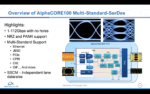
Over the recent years, the volume and velocity of discussions relating to chiplets have intensified. A major reason for this is the projected market opportunity. According to research firm Omdia, chiplets driven market is expected to be $6B by 2024 from just $645M in 2018. That’s an impressive nine-fold projected increase over… Read More
I mentioned back in June that Synopsys had launched a blog on formal verification, intended to demystify the field and provide help in understanding key concepts. It’s been a few months, time to check in on some of their more recent posts.
First up, it feels like they are finding their groove. Relaxed style, useful topics but now with… Read More
FPGA-based prototyping has provided a major advance in verification and validation for complex hardware/software systems but even its most fervent proponents would admit that setup is not exactly push-button. It’s not uncommon to hear of weeks to setup a prototype or of the prototype finally being ready after you tape-out. … Read More
It’s been a busy few days here in Canyon Lake, and we’re ready to share exciting news in advance of #53DAC coming up on Monday, June 6[SUP]th[/SUP]. S2C is offering a technical program tutorial on “Overcoming the Challenges of FPGA Prototyping” followed by the launch of our latest book project, “PROTOTYPICAL”, including a field… Read More
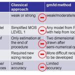
Digital designers have used logic optimization and logic synthesis for decades as a means to produce more optimal designs with EDA tools. On the analog and transistor-level side of design the efforts to automatically optimize for speed or power have generally been limited to circuits with only a handful of transistors. These … Read More
I was at DesignCon in Santa Clara today and listened to Jonah Alben of NVIDIA’s keynote on what their approach is to improving design methodology. He started by pointing out that most companies underinvest in EDA (and he includes NVIDIA in this). Partially it is complaceny: that last chip taped out so we know we can do it again.… Read More
Part I (here) looked at a bit of the history of scripting, makefiles and other approaches to more formally specify and institutionalize EDA design flows.
The most sophisticated tool I know that looks at this issue is RTDA’s FlowTracer.… Read More