Last week I went to a lunch and learn at Mentor about their Questa formal product given by Kurt Takara. Like everyone else these days, Questa is packaged as a number of Apps for doing different tasks. Formal verification is different from other EDA tools in that different approaches can be used for different sub-tasks. There are three… Read More
Tag: mentor
Temperature – The Fourth Aspect to Look at in SoC Design
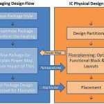
In my career in semiconductor industry, I can recall, in the beginning there was emphasis on design completion with automation as fast as possible. The primary considerations were area and speed of completion of a semiconductor design. Today, with unprecedented increase in multiple functions on the same chip and density of the… Read More
Wally Rhines at #51DAC: EDA Grows From Solving New Problems
Wally Rhines gave the keynote at DAC in 2004. One of the things that he pointed out ten years ago was that EDA revenue for any given market segment is pretty much flat once the initial growth phase has taken place and the market has been established. Incremental EDA revenue only comes from delivering new capabilities. Historically… Read More
The Secret Essence of an IoT Design
Today the semiconductor industry along with electronics industry is looking up to capitalize from massive expansion foreseen in IoT (Internet of Things) domain. In simple terms we can consider IoT as connectivity between machines which can communicate with each other and work as programmed. In localized applications such … Read More
Intel Invests in the Fabless Ecosystem!
During my illustrious career one of the most useful axioms that I use just about everyday day is: “Understand what people say but also understand why they are saying it.” This certainly applies to press releases so let’s take a look at what Intel unleashed during #51DAC (in alphabetical order):
ANSYS And Intel Collaborate… Read More
Automotive Focus @ #51DAC!
For the first time in DAC history there is an automotive track. Being a car person myself this is exciting news. I had a quick chat with Anne Cirkel, Vice Chair of DAC, and she sent me the following information to get us prepared for our week in San Francisco. The weather is going to be great so plan accordingly!
Ever increasing feature… Read More
Taming The Challenges of SoC Testability
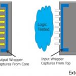
With the advent of large SoCs in semiconductor design space, verification of SoCs has become extremely challenging; no single approach works. And when the size of an SoC can grow to billions of gates, the traditional methods of testability of chips may no longer remain viable considering the needs of large ATPG, memory footprint,… Read More
The Matrix, your ultimate OPC
One of the many consequences of shrinking process nodes is that traditional OPC can no longer achieve good pattern fidelity with reasonable turn-around-time. But there is a solution; we made it ourselves and call it matrix OPC.
First, let’s explore the problems with traditional optical proximity correction (OPC) when applied… Read More
What Do You Do When You Are Not Designing?
DAC is coming up in a month (OMG less than 4 weeks and we are so not ready I hear a hundred marketing people cry out). That gives you four weeks (and a couple of days) to tell Mentor what you do in your spare time that you are passionate about (spare time, I hear a hundred engineers cry out, what is that?) and you could win $300.
For DAC, Mentor… Read More
FinFET & Multi-patterning Need Special P&R Handling
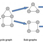
I think by now a lot has been said about the necessity of multi-patterning at advanced technology nodes with extremely low feature size such as 20nm, because lithography using 193nm wavelength of light makes printing and manufacturing of semiconductor design very difficult. The multi-patterning is a novel semiconductor manufacturing… Read More


