Mentor Graphics acquired Berkeley Design Automation this morning. The details of the deal were unannounced. This is a strong move by Mentor to challenge Cadence and Synopsys in the nanometer analog/mixed-signal market and nanometer memory characterization market, respectively. Mentor not only acquires the technology and… Read More
Tag: mentor graphics
Speeding Up AMS Verification by Modeling with Real Numbers
My first introduction to modeling an AMS behavior using a language was back in the 1980’s at Silicon Compilers using the Lsim simulator. Around the same time the VHDL and Verilog languages emerged to handle the modeling of both digital and some analog behaviors. The big reason to model analog behavior with a language is for… Read More
Stop TDDB from getting through peanut butter
There are a few dozen causes of semiconductor failure. Most can be lumped into one of three categories: material defects, process or workmanship issues, or environmental or operational overstress. Even when all those causes are carefully mitigated, one factor is limiting reliability more as geometries shrink – and it… Read More
An Update on the OpenPDK for IC Design
IC designers use EDA tools to implement their logical and physical design, and these tools require foundry-specific information for:
- Design Rule Checking (DRC)
- Layout Versus Schematic (LVS)
- Library Symbols
- Parasitic EXtraction (PEX)
Mastering the Magic of Multi-Patterning
I’ve been quite impressed that modern ICs use a lithography process with 193nm light sources to resolve final feature sizes at 20nm and smaller dimensions. We’ve been blogging about Double Patterning Technology (DPT) some 45 times in the past few years that enable 20nm fabrication, so one big question for me is, “How… Read More
Capturing Analog Design Intent with Verification
Analog IC designers are gradually adopting what digital IC designers have been doing for years, metric driven verification. When you talk with analog designers about their methodology and approach, you hear terms like artisan being used which implies mostly a manually-oriented methodology. Thanks to automation from EDA companies,… Read More
Bringing EDA to India
Why do all three big EDA companies have user group meetings in India? The answer is to grow the EDA market in India because so many multi-national companies have engineers in India doing SoC, and IP design work. In my 35 years of IC design and EDA experience I’ve had the pleasure of working with and knowing many engineers and managers… Read More
Social Media at Mentor Graphics
You can often tell how important blogging and social media is to an EDA company by how much effort it takes to find their blog from the Home page. For the folks at Mentor Graphics I’d say that blogging is quite important, because it shows up as a top-level menu item. Notice also how important Twitter is, their latest tweets show… Read More
Assertions verifying blocks to systems at Broadcom
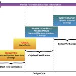
Speaking from experience, it is very difficult to get an OEM customer to talk about how they actually use standards and vendor products. A new white paper co-authored by Broadcom lends insight into how a variety of technologies combine in a flow from IP block simulation verification with assertions to complete SoC emulation with… Read More
A Hybrid Test Approach – Combining ATPG and BIST
In the world of IC testability we tend to look at various approaches as independent means to an end, namely high test coverage with the minimum amount of test time, minimum area impact, minimum timing impact, and acceptable power use. Automatic Test Pattern Generation (ATPG) is a software-based approach that can be applied to any… Read More


