As semiconductor manufacturing pushes deeper into the nanometer regime, computational lithography has evolved from a supporting step into a central pillar of advanced chip design. Mask synthesis, lithography simulation, and optical proximity correction (OPC) now demand unprecedented levels of accuracy and computational… Read More

Tag: lithography
TSMC Process Simplification for Advanced Nodes

In the modern world, the semiconductor industry stands at the heart of technological innovation. From smartphones and laptops to advanced medical devices and artificial intelligence systems, nearly every piece of contemporary electronics depends on increasingly sophisticated microchips. Among the leading companies … Read More
CEO Interview with Dr. Heinz Kaiser of Schott

With over 25 years of experience in the specialty materials industry, Dr. Heinz Kaiser is a member of the Management Board of SCHOTT AG, responsible for High-Performance Materials and Flat Glass, while also heading Sales and Market Development, Sales Excellence, and Intellectual Property. With a strong engineering background… Read More
Kirin 9030 Hints at SMIC’s Possible Paths Toward >300 MTr/mm2 Without EUV
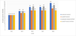
Earlier this month, TechInsights did a teardown of the Kirin 9030 chip found in Huawei’s Mate 80 Pro Max [1]. Two clear statements were made on the findings: (1) the transistor density of SMIC’s “N+3” process was definitely below that of the earlier 5nm processes from Samsung and TSMC, and (2) metal pitch was aggressively scaled
Self-Aligned Spacer Patterning for Minimum Pitch Metal in DRAM
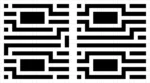
The patterning of features outside a DRAM cell array can be just as challenging as those within the array itself [1]. The array contains features which are densely packed, but regularly arranged. On the other hand, outside the array, the minimum pitch features, such as the lowest metal lines in the periphery for the sense amplifier… Read More
EUV Resist Degradation with Outgassing at Higher Doses
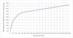
Dosing for EUV lithography walks a fine line between productivity and defectivity. Fabs can choose higher-dose exposures to suppress photon shot noise [1]. However, higher doses require EUV machines to scan the wafer at slower speeds, degrading throughput [2].
On the other hand, there is the threat of resist thickness loss that… Read More
Impact of Varying Electron Blur and Yield on Stochastic Fluctuations in EUV Resist

A comprehensive update to the EUV stochastic image model
In extreme ultraviolet (EUV) lithography, photoelectron/secondary electron blur and secondary electron yield are known to drive stochastic fluctuations in the resist [1-3], leading to the formation of random defects and the degradation of pattern fidelity at advanced
Stitched Multi-Patterning for Minimum Pitch Metal in DRAM Periphery
In a DRAM chip, the memory array contains features which are the most densely packed, but at least they are regularly arranged. Outside the array, the regularity is lost, but in the most difficult cases, the pitches can still be comparable with those within the array, though generally larger. Such features include the lowest metal… Read More
Variable Cell Height Track Pitch Scaling Beyond Lithography
Two approaches compared
With half-pitch approaching 10 nm, EUV patterning is heavily impacted by stochastic effects, which are aggravated from reduced image contrast from electron blur [1]. A two-mask (“LELE”: Litho-Etch-Litho-Etch) approach was proposed to pattern core features for self-aligned double patterning (SADP)… Read More
A Realistic Electron Blur Function Shape for EUV Resist Modeling
Peak probability at zero distance actually makes no sense
In lithography, it is often stated that the best resolution that can be achieved depends on wavelength and numerical aperture (NA), but this actually only applies to the so-called “aerial” image. When the image is actually formed in the resist layer, it also depends on an… Read More