You are currently viewing SemiWiki as a guest which gives you limited access to the site. To view blog comments and experience other SemiWiki features you must be a registered member. Registration is fast, simple, and absolutely free so please,
join our community today!
Dan is joined by Dr. Julien Ryckaert who joined imec as a mixed-signal designer in 2000, specializing in RF transceivers, ultra-low power circuit techniques, and analog-to-digital converters. In 2010, he joined imec’s process technology division in charge of design enablement for 3DIC technology. Since 2013, he oversees… Read More
It lays the foundation for the Stochastics Resolution Gap
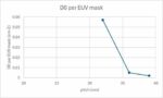
Chris Mack, the CTO of Fractilia, recently wrote of the “Stochastics Resolution Gap,” which is effectively limiting the manufacturability of EUV despite its ability to reach resolution limits approaching 10 nm in the lab [1,2]. As researchers have inevitably found, … Read More
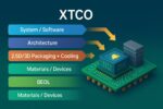
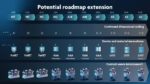
imec XTCO (Cross-Technology Co-Optimization) is the natural successor to DTCO and STCO in an era where no single layer of the stack can deliver scaling alone. Instead of optimizing devices, interconnect, packaging, architecture, and software in isolation, XTCO treats them as one tightly coupled system with a shared budget … Read More
At #61DAC our very own Daniel Nenni from SemiWiki moderated an informative panel discussion on the topic of 3D IC Design Ecosystem. Panelists included: Deepak Kulkarni – AMD, Lalitha Immaneni – Intel Foundry, Trupti Deshpande – Qualcomm, Rob Aitken – CHIPS, Puneet Gupta – UCLA, Dragomir Milojevic – imec. Each panelist had a brief… Read More
– We just finished the most happy SEMICON West in a long time
– IMEC stole the show- HBM has more impact than size dictates
– Has Samsung lost its memory mojo? Is SK the new leader?
– AI brings new tech issues with it – TSMC is still industry King
Report from SEMICON West
The crowds at Semicon West were both… Read More
At IEDM 2023, Naoto Horiguchi presented on CFETs and Middle of Line integration. I had a chance to speak with Naoto about this work and this write up is based on his presentation at IEDM and our follow up discussion. I always enjoy talking to Naoto, he is one of the leaders in logic technology development, explains the technology in … Read More
Harry Peterson is a mixed-signal chip designer with a BS in Physics from Caltech. He managed IC design groups within Fairchild, Kodak, Philips, Northern Telecom, Toshiba and Pixelworks. During sabbaticals he helped fly experiments on NASA’s orbiting satellite observatory (OSO-8) and build telescopes in the Canary… Read More
The SPIE Advanced Lithography Conference was held in February. I recently had the opportunity to interview Steven Scheer, vice president of advanced patterning process and materials at imec and review selected papers that imec presented.
I asked Steve what the overarching message was at SPIE this year, he said readiness for … Read More
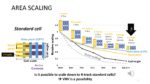
At the IEDM conference in December 2022, Imec presented “Semi-damascene Integration of a 2-layer MOL VHV Scaling Booster to Enable 4-track Standard Cells,” I had a chance to not only read the paper and see it presented, but also to interview one of the authors Zsolt Tokie.
Logic designs are built up by standard cells such as inverters,… Read More
SEMICON West 2022 was held from July 12th to 14th at the Moscone Center in San Francisco.
On Monday the 11th before the show, Imec held a technology forum at the Marriott Marquee right around the corner from the Moscone center. In recent years the Imec forums have shifted away from the process technology I cover to more of a system and… Read More