You are currently viewing SemiWiki as a guest which gives you limited access to the site. To view blog comments and experience other SemiWiki features you must be a registered member. Registration is fast, simple, and absolutely free so please,
join our community today!
Coming up on April 10th is the SEMI Silicon Valley Breakfast Forum Internet of Things—Driving the Microelectronics Revolution. It runs from 7am to 10.45am and will be held at SEMI Headquarters which is at 3081 Zanker Road in San Jose.
Widespread adoption of the Internet of Things will take time, but the movement is advancing thanks… Read More
Whenever there is good momentum in a particular technology, IEEEtakes major initiative to standardize the procedures, formats, methods, measurements etc. involved in the technology to proliferate it for the advantage of wider community. And that becomes successful by active participation and collaboration of both producers… Read More
In case you haven’t noticed, Synopsys has been in the press lately talking about their relationship with TSMC. Since I’m an internationally recognized industry expert they gave me a call for a briefing and I was happy to do it. Staying connected with the #1 EDA company is important and fun since I get to ask questions that most people… Read More
At ICCAD earlier this week, CEDA sponsored a talk by Alberto Sangiovanni-Vincentelli looking back over the last 30 years (it is the 30th anniversary of ICCAD) and looking to the future. As is always the case in these sorts of presentations, the retrospective contained a lot more detail than the going forward part. Clayton Christensen… Read More
What can we do for Earth’s sustainability? Besides sorting our garbage and recycling our lawn clippings? Sustainability must be the paramount theme for the future of human society! Semiconductors for a better life! Well, according to my kids, if you take away their smart phones there is no life!… Read More
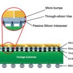
When process nodes reached 28 nm and below, it appeared that design density is reaching a saturation point, hitting the limits of Moore’s law. I was of the opinion that the future of microelectronic physical design was limited to 20 and 14 nm being addressed by technological advances such as FinFETs, double patterning, HKMG (High-k… Read More
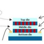
The IEEE has an Orange Country Chapter of the Components, Packaging and Manufacturing Technology Society who are organizing an all-day workshop, 3D Integrated Circuits: Technologies Enabling the Revolution. This looks to be an informative day with real-world examples in both design and test being presented by over a dozen … Read More