You are currently viewing SemiWiki as a guest which gives you limited access to the site. To view blog comments and experience other SemiWiki features you must be a registered member. Registration is fast, simple, and absolutely free so please,
join our community today!
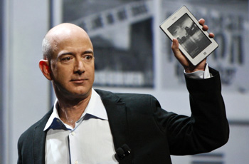
In the world of Tech Goliaths, the seemingly low tech, not for profit Amazon continues to amaze investors with a high and rising stock price. More so than Google, Amazon is considered to have retail all wrapped up with the end game being sky-high warehouses and continuous truck rolls up and down our scenic neighborhoods. Walmart … Read More
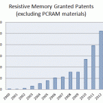
(with apologies to George Harrison) Two recent Blogs over at ReRAM-Forum.com have focused on the latest in the IP field, particularly as it affects resistive memory. A high level overview of who is patenting what suggests a healthy amount of R&D is going on in the field. But looking a little deeper suggests there is much overlap… Read More
“Innovations for Next Generation Scaling”
The 2013 Forum today (Feb 5, 2013) started with a presentation by Dr. Gary Patton, VP, IBM Semiconductor Research & Development Center. Gary very clearly articulated the two irresolvable challenges the industry now faces:
- On chip interconnect
- Lithography
These … Read More
I was at the Common Platform Technology Forum this week. One of the most interesting sessions is IBM’s Gary Patton giving an overview of the state of semiconductor fabrication. Then, at lunchtime, he is one of the people that the press can question. In this post, I’m going to focus on Extreme Ultra-Violet (EUV) lithography.… Read More
Can’t make it to Santa Clara? Join us online!
The detailed 2013 CPTF agenda is now up in preparation for the February 5th event at the Santa Clara Convention Center. This is one of the rare times that you can get a free lunch! Watch this quick video to see what is in store for us this year. Dr. Paul McLellan and I will be there so please… Read More
GLOBALFOUNDRIES changed the landscape of the foundry business in 2009 with a simple but ambitious plan to become the world’s first truly global foundry. At the Common Platform Technology Forum February 5th in the Santa Clara Convention Center GF Executive Vice President Michael Noonen will give an update on how that is … Read More
The Common Platform Alliance — IBM, Samsung Electronics, Co., Ltd., and GLOBALFOUNDRIES — continues to redefine the landscape of the semiconductor industry with its groundbreaking collaboration. Join us at our 2013 Common Platform Technology Forumon Tuesday, February 5, 2013 at the Santa Clara Convention Center as we showcase… Read More
An announcement at the ARM conference was of a joint project to tape out an ARM Cortex-M0 in IBM’s 14nm FinFET process. In fact they taped out 3 different versions of the chip using different routing architectures to see the impact on yield.
This was the first 14nm ARM tapeout, it seems. I’m sure Intel has built plenty … Read More
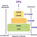
The recent (August) flash memory summit in Santa Clara had a session devoted to ReRAM as well as featuring prominently in the keynote address by Sung Wook Park of SK Hynix. The talk includes a summary of NAND’s well known scaling issues along with approaches to 3D NAND. It turns out that they are working on three different technologies:… Read More
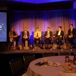
Wednesday morning I attended a panel discussion with: ARM, IBM, Cadence, GLOBALFOUNDRIES and Samsung.
The panelists all sang the same song of collaboration between EDA, IP and Foundry to enable 28nm, 20nm and even 14nm.… Read More