You are currently viewing SemiWiki as a guest which gives you limited access to the site. To view blog comments and experience other SemiWiki features you must be a registered member. Registration is fast, simple, and absolutely free so please,
join our community today!
So where in the world do you think semiconductor manufacturing is increasing the fastest? OK, Taiwan, that was pretty easy. But in second place, with over 20% of the world’s semiconductor equipment capital investment is the US. Growing faster than Europe, China, Japan and equal with Korea.
This was not the case half a dozen… Read More
Global Foundries will be at DAC in booth 1314. There will be 6 pods there demonstrating:
- Advanced Technology: 28nm ready and ramping, and next is 20LPM and 14XM.
- PDKs: For 28nm, 20nm and 14nm. 14nm handles FinFET enablement complexity. Robust, easy to use and high quality, supports pretty much the full range of EDA tools.
- Design
…
Read More
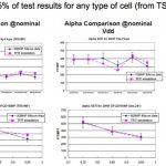
I blogged last month about single event effects (SEE) where a semiconductor chip behaves incorrectly due to being hit by an ion or a neutron. Since we live on a radioactive planet and are bombarded by cosmic rays from space, this is a real problem, and it is getting worse at each process node. But just how big of a problem is it?
TFIT is … Read More
Can’t make it to Santa Clara? Join us online!
The detailed 2013 CPTF agenda is now up in preparation for the February 5th event at the Santa Clara Convention Center. This is one of the rare times that you can get a free lunch! Watch this quick video to see what is in store for us this year. Dr. Paul McLellan and I will be there so please… Read More
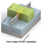
I spent some quality time with Subi Kengeri, Vice President, Technology Architecture, Office of the CTO, GLOBALFOUNDRIES in Las Vegas during CES. Great guy, he worked at Silicon Access, Virage and TSMC before GF. One thing you should know about embedded memory guys, SRAM is the first thing that goes through a new process so they … Read More
GLOBALFOUNDRIES changed the landscape of the foundry business in 2009 with a simple but ambitious plan to become the world’s first truly global foundry. At the Common Platform Technology Forum February 5th in the Santa Clara Convention Center GF Executive Vice President Michael Noonen will give an update on how that is … Read More
In my opinion, FinFETs will be the most significant piece of technology we, as semiconductor ecosystem people, will experience this decade. Seriously this is exciting stuff and one of the top search terms on SemiWiki for 6 months running. Here is a quick peek at what the top EDA companies will be talking about at the Common Platform… Read More
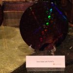
Incredibly exciting! Even my beautiful wife was impressed by the rainbow of colors it reflected. From left to right: 28nm, 20nm, and 14nm wafers. The 20nm and 14nm wafers are from the GLOBALFOUNDRIES NY fab, made in the USA! GF also announced another $3-4B CAPEX for 2013 to increase capacity of all three of their 300mm fabs (Singapore,… Read More
Time to pack up for the 2013 Consumer Electronics Show in Las Vegas, I will be driving down with my beautiful wife Shushana because she does not like to fly. The drive takes the better part of a day so we will leave early and see the sunrise over the desert. She is great company, the time will fly by. We will be 2 of the more than 150,000 people… Read More
The Common Platform Alliance — IBM, Samsung Electronics, Co., Ltd., and GLOBALFOUNDRIES — continues to redefine the landscape of the semiconductor industry with its groundbreaking collaboration. Join us at our 2013 Common Platform Technology Forumon Tuesday, February 5, 2013 at the Santa Clara Convention Center as we showcase… Read More