You are currently viewing SemiWiki as a guest which gives you limited access to the site. To view blog comments and experience other SemiWiki features you must be a registered member. Registration is fast, simple, and absolutely free so please,
join our community today!
Part 1 here.
The line between fabless semiconductor companies and IDMs has blurred over the last decade. Back in the 1990s, most IDMs manufactured most of their own product, perhaps using a foundry for a small percentage of additional capacity when required. But their own manufacturing was competitive, both in terms of the capacity… Read More
The fundamental economics of the semiconductor industry are summed up in the phrase “fill the fab.” Building a fab is a major investment. With a lifetime of just a few years, the costs of owning a fab are dominated by depreciation of the fixed capital assets (the building, the air and water purification equipment, the manufacturing… Read More
In the 1980s, Japan was seen as the leader in the semiconductor industry. Their quality was higher, especially in memories, and the US was worried about falling behind. In fact Sematech was created in 1987 by the US government and a consortium of 14 US-based semiconductor companies primarily to pool investment on common problems… Read More
As an investor, one has to always be aware when Jim Cramer informs the world of the investment scenario you have been playing comes out of the shadows and sees the light of day. Soon the herd will follow which is positive, but now one has to figure how long to ride the roller coaster. In an article posted on thestreet.com entitled “Tech… Read More
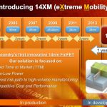
Today GlobalFoundries announced a 14nm process that will be available for volume production in 2014. They are explicitly trying to match Intel’s timeline for the introduction of 14nm. The process is called 14XM for eXtreme Mobility since it is especially focused on mobile. The process will be introduced just one year after… Read More
I went to a couple more sessions at the Common Platform Technology Forum today, on 20nm double patterning and whatever will we do at 14nm. Basically, this is the end of planar transistors and the end of optical lithography. One session was by IBM scientists about process and one by Michael White of Mentor about double patterning. … Read More
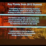
There were keynotes from all three semiconductor partners in the Common Platform Alliance and, as if to show how common they are, they all talked about the problems that need to be addressed in the next decade and a half and they all said pretty much the same thing. Gary Patton of IBM went first and so he got to say everything first. Plus,… Read More
Next Wednesday is the Common Platform Technology Forum. “Common Platform” is a name that only a committee could have come up with, giving no clue as to what it actually is. As you probably know, there are various process clubs sharing the costs of technology development (TD) and one of them consists of IBM, Samsung and… Read More
The CEO panel at the 2nd GTC wasn’t especially enlightening. The theme was that going forward will require cooperation for success and everyone was really ready to cooperate.
The most interesting concept was Aart talking about moving from what he called “scale complexity” aka Moore’s law to what he … Read More
I went to the second Global Technology Conference yesterday. It started with a keynote by Ajit Manocha who is the CEO of about 2 months. I hadn’t realized until someone asked him during the press lunch that he is technically only the “acting” CEO. Actually, given his experience he might be the right person anyway,… Read More