On a DRAM chip, the patterning of features outside the cell array can be just as challenging as those within the array itself. While the array contains features which are the most densely packed, at least they are regularly arranged. On the other hand, outside the array, the regularity is lost, but the in the most difficult cases, … Read More

Tag: Fred Chen
Predicting Stochastic Defectivity from Intel’s EUV Resist Electron Scattering Model
The release and scattering of photoelectrons and secondary electrons in EUV resists has often been glossed over in most studies in EUV lithography, despite being a fundamental factor in the image formation. Fortunately, Intel has provided us with a laboriously simulated electron release and scattering model, using the GEANT4… Read More
The Significance of Point Spread Functions with Stochastic Behavior in Electron-Beam Lithography
Electron beam lithography is commercially used to directly write submicron patterns onto advanced node masks. With the advent of EUV masks and nanometer-scale NIL (nanoimprint lithography), multi-beam writers are now being used, compensating the ultralow throughput of a single high-resolution electron beam with the use… Read More
Extension of DUV Multipatterning Toward 3nm
China’s recent achievement of a 7nm-class foundry node using only DUV lithography [1] raises the question of how far DUV lithography can be extended by multipatterning. A recent publication at CSTIC 2023 indicates that Chinese groups are currently looking at extension of DUV-based multipatterning to 5nm, going so far… Read More
Stochastic Model for Acid Diffusion in DUV Chemically Amplified Resists
Recent articles have focused much effort on studying the stochastic behavior of secondary electron exposure of EUV resists [1-4]. Here, we consider the implications of extending similar treatments to DUV lithography.
Basic Model Setup
As before, the model uses pixel-by-pixel calculations of absorbed photon dose, followed… Read More
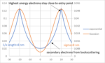
Modeling EUV Stochastic Defects with Secondary Electron Blur
Extreme ultraviolet (EUV) lithography is often represented as benefiting from the 13.5 nm wavelength (actually it is a range of wavelengths, mostly ~13.2-13.8 nm), when actually it works through the action of secondary electrons, electrons released by photoelectrons which are themselves released from ionization by absorbed… Read More
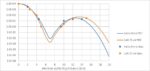
Assessing EUV Wafer Output: 2019-2022
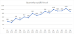
At the 2023 SPIE Advanced Lithography and Patterning conference, ASML presented an update on its EUV lithography systems in the field [1]. The EUV wafer exposure output was presented and is shown below in table form:
From this information, we can attempt to extract and assess the EUV wafer output per quarter. First, since there … Read More
Horizontal, Vertical, and Slanted Line Shadowing Across Slit in Low-NA and High-NA EUV Lithography Systems
EUV lithography systems continue to be the source of much hope for continuing the pace of increasing device density on wafers per Moore’s Law. Recently, although EUV systems were originally supposed to help the industry avoid much multipatterning, it has not turned out to be the case [1,2]. The main surprise has been the
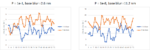
Revisiting EUV Lithography: Post-Blur Stochastic Distributions
In previous articles, I had looked at EUV stochastic behavior [1-2], primarily in terms of the low photon density resulting in shot noise, described by the Poisson distribution [3]. The role of blur to help combat the randomness of EUV photon absorption and secondary electron generation and migration was also recently considered… Read More
Calculating the Maximum Density and Equivalent 2D Design Rule of 3D NAND Flash
I recently posted an insightful article [1] published in 2013 on the cost of 3D NAND Flash by Dr. Andrew Walker, which has since received over 10,000 views on LinkedIn. The highlight was the plot of cost vs. the number of layers showing a minimum cost for some layer number, dependent on the etch sidewall angle. In this article, the same… Read More