I think we can all agree that no matter what you are designing, FPGA prototyping can help. The challenge is getting the most out of the leading edge FPGA prototyping solutions and that requires a detailed understanding of how this technology works and what FPGA prototyping solutions match your design and verification requirements.… Read More

Tag: fpga prototyping
S2C’s Virtex UltraScale Prototyping Provides Designers Much Needed Flexibility
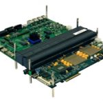
The advent of large system-on-chip (SoC) designs has brought FPGA prototyping hardware into the limelight and the launch of S2C Inc.’s Single VU440 Prodigy Logic Module just shows how far off-the-shelf prototyping has come in a bid to complement hardware verification and software development. Hardware verification… Read More
A Vision for FPGA Prototyping Realized
FPGA prototyping is beginning its move to the forefront of design and verification. More and more companies are turning to this technology not only for in-circuit testing and earlier software development but also for refining, validating, and implementing chip architecture. The increases in design size and complexity as well… Read More
Prototyping Over 100 Million ASIC Gates Capacity
Most SoCs today are being prototyped in FPGA hardware before committing to costly IC fabrication. You could just design and build your own FPGA prototyping system, or instead choose something off the shelf and then concentrate on your core competence of SoC design.
Thanks to the FPGA vendors like Xilinx we now have FGPA prototyping… Read More
ASIC Prototyping: Dini Group and Tektronix
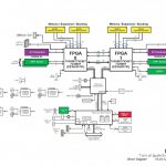
Collaboration in EDA is nothing new, however you may not be aware of how the Dini Group and Tektronix have worked together on an FPGA prototyping platform to address issues like debugging with full visibility across an entire multi-FPGA design. At SemiWiki we’ve blogged a couple of times so far about the new debug approach… Read More
What I Learned About FPGA-based Prototyping
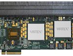
Today I attended an Aldec webinar about ASIC and SoC prototyping using the new HES-7 Board. This prototyping board is based on the latest Virtex-7 FPGA chips from Xilinx.
You can view the recorded webinar here, which takes about 30 minutes (should be available in a few days). I first blogged about the HES-7 two months ago, ASIC Prototyping… Read More
Embedding 100K probes in FPGA-based prototypes
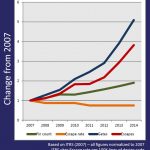
As RTL designs in FPGA-based ASIC prototypes get bigger and bigger, the visibility into what is happening inside the IP is dropping at a frightening rate. Where designers once had several hundred observation probes per million gates, those same several hundred probes – or fewer if deeper signal captures are needed – are now spread… Read More
FPGA Prototyping – What I learned at a Seminar

Intro
My first exposure to hardware prototyping was at Intel back in 1980 when the iAPX 432 chip-set group decided to build a TTL-based wire-wrap prototype of a 32 bit processor to execute the Ada language. The effort to create the prototype took much longer than expected and was only functional a few months before silicon came back.… Read More