You are currently viewing SemiWiki as a guest which gives you limited access to the site. To view blog comments and experience other SemiWiki features you must be a registered member. Registration is fast, simple, and absolutely free so please,
join our community today!
Triple Patterningby Paul McLellan on 03-19-2014 at 1:00 pmCategories: EDA, Foundries
As you can’t have failed to notice by now, 28nm is the last process node that does not require double patterning. At 20nm and below, at least some layers require double patterning. The tightest spacing is typically not the transistors but the local interconnect and, sometimes, metal 1.
In the litho world they call double patterning… Read More
As I see the semiconductor industry going through significant changes and advances, yet ironically plagued by a growing perception that the pace of scaling is slowing, I was inclined to take a peek into what the industry experts say about the state of the industry and the future of Moore’s Law. Fortunately, at last week’s International… Read More
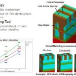
The growing process integration complexity at each technology node has increased development time and cost, and this trend looks to continue. There is a looming risk of delivering unrepeatable critical unit processes (or process modules) that would require revisiting development and manufacturing requalification or in … Read More
Yes, it’s a pleasant surprise; it is Virtual Fabrication Platform, one of the new innovations in 2013. I was looking around for what kind of breakthrough technologies will be announced in DAC this year. And here I came across this new kind of innovative tool which can produce final virtual fabricated 3D structures after following… Read More


