You are currently viewing SemiWiki as a guest which gives you limited access to the site. To view blog comments and experience other SemiWiki features you must be a registered member. Registration is fast, simple, and absolutely free so please,
join our community today!
Atrenta will have a new look this year at DAC. I’m not quite sure what that means but we’ll all just have to go along and find out.
They have three users talking about their use of Atrenta’s tools. All 3 of these presentations are in the user-track poster session on Tuesday June 5th 12.30-1.30pm in room 105 (which … Read More
At DAC in San Francisco this year, Apache once again have a mixture of presentations by customers on their use of Apache tools and presentations by Apache themselves on their products. Most of the customer presentations are given just once, but the product presentations are given multiple times over the three days.
I think one of… Read More
Adding sophisticated 2D dynamic compaction technology to address 20nm and 14nm challenges. Santa Clara, California – May 3 ,2012 – Sagantec today announced that it has acquired Dutch startup NP-Komplete Technologies BV (Eindhoven, The Netherlands) for its physical design compaction and migration solutions based on a sophisticated… Read More
Now that the 28nm challenges are dead
It is time to look ahead
The tabloid pundits may not agree
But Moore’s law again you will see
The semiconductor ecosystem is humming
(2X gate density -20%+ performance-20%+ power savings)
The 20nm design starts are coming!
Okay, I’m really bad at poetry. Gambling however, I do pretty well. Las… Read More
The success of Apple’s AppStore has made people aware that software doesn’t have to be delivered in a big monolithic lump. Indeed, going back a bit earlier, Apple’s iTunes store made people aware that you didn’t have to buy a whole album if you only wanted a track or two.
EDA applications in today’s… Read More
In one of Portlandia’s TV program sketches, there is a funny interchange between a carrier salesperson and Fred Armisen (of SNL fame) who was trying to buy a phone. One chuckle line was a statement by the seller that the phone was free after paying for it and that there was a one-time annual fee. With this anecdote as a mental backdrop,… Read More
We are all aware that at 28nm and below several types of complex layout effects manifest themselves into the design and pose a herculean task, with several re-spins to correct them at pre-tapeout. It’s apparent that the layout needs to be correct by construction at the very beginning during the design stage.
Having worked at Cadence… Read More
There’s this EDA company. They have over 100 tapeouts. They have a $28M in funding. They have 250 people. And you’ve never heard of them. Or at least I hadn’t.
They are ICScape. They started in 2005 with an investment from Acorn Campus Ventures and delivered their first product, ClockExplorer, in 2007 and their… Read More
There is a famous quote (probably attributed to Mark Twain who gets them all by default) “When looking for faults use a mirror not a spyglass.” Of course if you have RTL of your IP or your design then using a SpyGlass is clearly the better way to go. But it is getting even better since there is a new enhanced release, SpyGlass… Read More
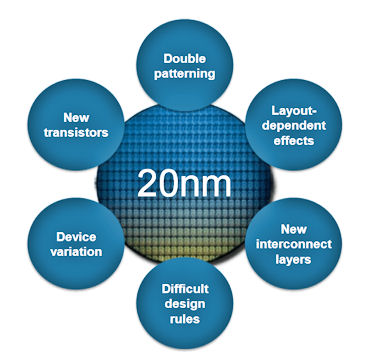
While the debate rages on about 28nm yield at foundry juggernaut TSMC, on Monday I attended a webinar on 20nm IC design hosted by TSMC and Synopsys. Double Patterning Technology (DPT) becomes a requirement for several layers of your 20nm IC design which then impact many of your EDA tools and methodology.… Read More