You are currently viewing SemiWiki as a guest which gives you limited access to the site. To view blog comments and experience other SemiWiki features you must be a registered member. Registration is fast, simple, and absolutely free so please,
join our community today!
My oldest son just upgraded Smart Phones from a 3″ display to a 4.5″ display and was shocked to discover that his battery barely lasted 8 hours, so I welcomed him to the reality of limited battery life in modern SoC-based mobile devices. There is some hope in increasing battery life for our consumer-oriented devices … Read More
Going to DAC? I just booked my plane ticket last weekend since flights from the Bay Area to wherever DAC is are so often overbooked. It’s in Austin this year in case you’ve been living under a rock. There are lots of reasons to go, from the academic conference to the world’s biggest EDA exhibition. And here is one … Read More
Jasper is presenting at both ends of the world at both ends of February.
First in Israel, it is SemiIsrael Verification Day 2013 on February 5th (next Tuesday) at Green House in Tel Aviv.
- Zihad Hanna, VP of Research and Chief Architect and General Manager of Jasper Israel will be talking about Security Formal Verification of Hardware
…
Read More
I already talked about how Cadence is splitting Virtuoso into two. Anyway, it is now officially announced. The 6.1 version will continue to be developed as a sort of Virtuoso classic for people doing designs off the bleeding edge that don’t require the new features. And a new Virtuoso 12.1 intended for people doing 20nm and… Read More
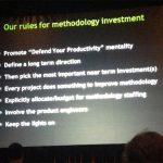
I was at DesignCon in Santa Clara today and listened to Jonah Alben of NVIDIA’s keynote on what their approach is to improving design methodology. He started by pointing out that most companies underinvest in EDA (and he includes NVIDIA in this). Partially it is complaceny: that last chip taped out so we know we can do it again.… Read More
While the SPIE Advanced Lithography conference is best known for IC manufacturing, computational lithography, mask preparation and other back-end topics, there is also a significant amount of interest in Design for Manufacturing (DFM) at the conference because some litho issues are best (or only) addressed by modifying the… Read More
While founder John Tanner, PhD, got his initial exposure to the TTL Cookbook and CMOS Cookbook as an undergraduate, it was his experience as a Caltech graduate student that forged his early path in EDA. In 1979, while enrolled in a VLSI design course at Caltech, John and his classmates received a pre-print of Carver Mead’s seminal… Read More
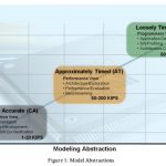
SoC designers have always wanted to simulate hardware and software together during new product development, so one practical question has been how to trade off performance versus accuracy when creating an early model of the hardware. The creative minds at Carbon Design Systems and ARM have combined to offer us some hope and relief… Read More
DesignConis next week in Santa Clara, so today I spoke with Mark Ravenstahlfrom ANSYS to get an idea of what to expect at the conference and trade show.
… Read More
Non-volatile memory is used in a wide variety of consumer and industrial applications and comes in an array of architectures like Serial Flash and CBRAM (Conductive Bridging RAM). I caught up with Shane Hollmer by phone this week to gain some insight into a recent acquisition of Atmel’s serial flash components, and how that… Read More