You are currently viewing SemiWiki as a guest which gives you limited access to the site. To view blog comments and experience other SemiWiki features you must be a registered member. Registration is fast, simple, and absolutely free so please,
join our community today!
A few weeks back I wrote an article mentioning that Mentor Graphics has been quietly working on solutions for photonic integrated circuits (PICs) for some time now, while one of their competitors has recently established a photonics beachhead. One of the most common challenges for PIC designs is their curvilinear nature, thus… Read More
A new world of 10nm design constraintsby Beth Martin on 08-30-2016 at 4:00 pmCategories: EDA, Siemens EDA
Every time the industry transitions to a smaller process node IC design software undergoes extensive updates.
I talked to a couple of experts in physical design at Mentor Graphics about what is involved in making place-and-route software ready for a new node. This is what I learned from Sudhakar Jilla, the IC design marketing director… Read More
After reading previous SemiWiki coverage on Dassault Systèmes and their ENOVIA Pinpoint solution, one big item seemed missing: how does this thing actually work? With all due respect to our other bloggers who covered when Dassault Systèmes acquired Pinpoint from Tuscany Design Automation, why Qualcomm is using Pinpoint, and… Read More
If you’ve followed my last article, The Guiding Light and Other Photonic Soaps, you read my comments about the use of waveguides to “guide the light” in photonic integrated circuits (PICs). This article continues the soap opera theme, this time with the Young and the Restless. My point here is that I am continually struck by the dichotomies… Read More
In the history of semiconductor design and manufacturing, the age-old concept of DRC rule-deck qualification for handshake between design and manufacturing still applies strongly to produce working silicon. In fact, DRC clean GDSII works as the de facto golden gate between a design and a foundry for manufacturing the chip for… Read More
Albert Einsteinhad said, “In the middle of difficulty lies opportunity”. In today’s world dominated by technology, or I must say internet which has initiated collaborative information sharing, “leading from the middle” is the new mantra of life.… Read More
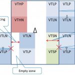
The market demanded that gadgets it loves become ever more conscious of their power consumption, and chip designers responded with an array of clever techniques to cut IC power use. Unsurprisingly, these new techniques added to the complexity of IC verification. When you’re verifying a design that has 100+ separate power domains,… Read More
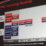
The technology for 10 nm is settled, but what about 7 nm and 5 nm? Those nodes will happen with silicon-based CMOS and 193nm immersion lithography, but exactly how is still being worked out. Right now, though, the focus is on getting 10 nm chips into high-volume production. TSMC and Intel both claim to be on track for high-volume manufacturing… Read More
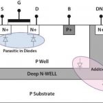
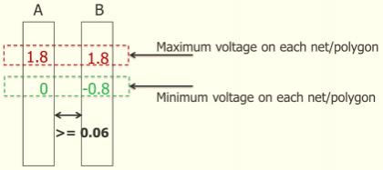
Because IC design and verification never gets simpler, verification engineers now have to comply with voltage-dependent DRC (VD-DRC) rules. What does this term mean, and what new challenges does it bring to the DRC task? I’d like to share what I learned during another water-cooler conversation with Dina Medhat, senior technical… Read More
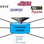
Design Rule Check (DRC) is the #1 foundry sign-off check. Fabless companies receive the DRC deck from the foundry; it’s a file comprising thousands of commands in a proprietary checker language for a specific DRC tool. In advanced technologies such a deck executes tens of thousands of geometric operations on the physical… Read More