You are currently viewing SemiWiki as a guest which gives you limited access to the site. To view blog comments and experience other SemiWiki features you must be a registered member. Registration is fast, simple, and absolutely free so please,
join our community today!
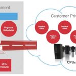
Over the years DRC tools have done an admirable job of keeping pace with the huge growth of IC design size. Yet, DRC runs for sign off on the full design using foundry rule decks take many hours to complete. These long run times are acceptable for final sign off, but there are many situations where DRC results are needed quickly when small… Read More
This area of automating the design of Flat Panel Displays (FPD) is so broad that it has taken me three blogs to cover all of the details, so in brief review the first two blogs were:
My final blog covers five areas:
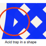
- DRC/LVS for curvilinear layout
- Circuit
…
Read More
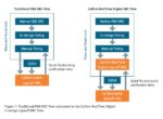
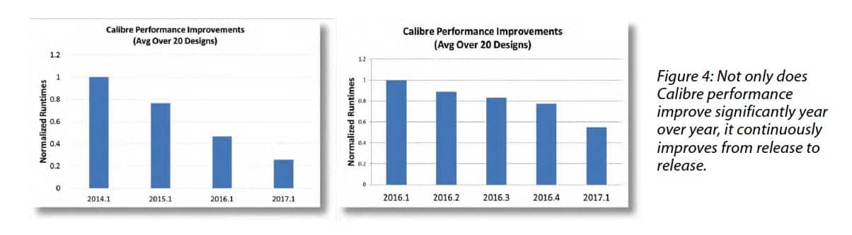
Calibre was a big game changer for DRC users when it first came out. Its hierarchical approach dramatically shortened runtimes with the same accuracy as other existing, but slower, flat tools. However, one unsung part of this story was that getting Calibre up and running required minimal effort for users. Two things are required… Read More
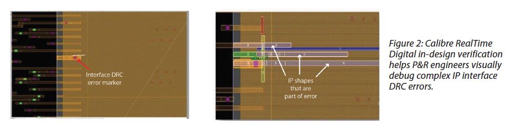
When floor planning (FP) and place & route (P&R) tools took over from custom layout tools for standard cell based designs, life became a lot better for designers of large digital chips. The beauty of the new flows was that all the internals of the standard cells and many IP blocks were hidden from view, lightening the load … Read More
Functional and physical verification are easily the two long poles in most IC product developments. During a design implementation cycle, design teams tend to push physical verification (PV) step towards the end as it is a time consuming process and requires significant manual interventions.
PV Challenges
In the traditional… Read More
Design process retargeting is acommon recurrence based on scaling orBOM(Bill-Of-Material) cost improvement needs. This occursnot only with the availability of foundry process refresh to a more advanced node,but also to any new derivative process node tailored towards matching design complexity, power profile or reliability… Read More
Being new in Ottawa and trying to get some momentum towards automation in full custom layout I was telling industry people that I am interested to work with everybody to move this agenda forward. My Director of Engineering at that time, Peter Gillingham, took me to visit Carleton University in Ottawa. One of his professor friends,… Read More
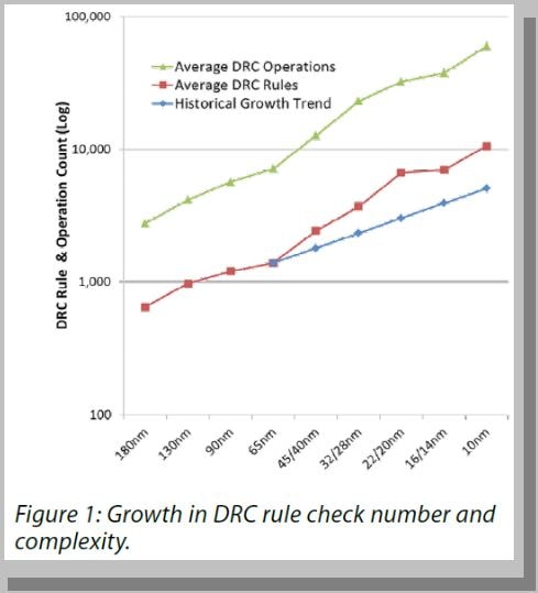
One might be tempted to think that technology driven gains in computer performance might be enough to keep up with the needs of design and verification tools. We know that design complexity is increasing at a rate predicted by Moore’s Law. We also know that the performance of the computers used during IC development benefit from … Read More
Chip designers are familiar with the additional physical design checking requirements that were incorporated into flows at advanced process nodes. With the introduction of optical correction and inverse lithography technology applied during mask data generation, and with the extension of a 193nm exposure source to finer… Read More
Back in the day the Dracula tool from Cadence was king of the DRC and LVS world for physical IC verification, however more recently we’ve seen Calibre from Mentor Graphics as the leader in this realm. Cadence wanted to reclaim their earlier prominence in physical verification so they had to come out with something different… Read More