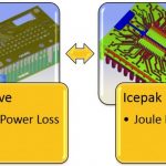
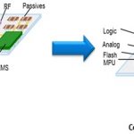
2015 will be remembered as the year when chip-package-system (CPS) physical co-design and electrical/thermal analysis methodologies took center stage.… Read More
Tag: ctm
ANSYS Enters the League of 10nm Designs with TSMC
The way we are seeing technology progression these days is unprecedented. It’s just about six months ago, I had written about the intense collaboration between ANSYSand TSMCon the 16nm FinFET based design flow and TSMC certifying ANSYS tools for TSMC 16nm FF+ technology and also conferring ANSYS with “Partner of the Year” award.… Read More
FinFET Designs Need Early Reliability Analysis
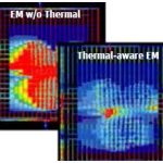
In a world with mobile and IoT devices driven by ultra-low power, high performance and small footprint transistors, FinFET based designs are ideal. FinFETs provide high current drive, low leakage and high device density. However, a FinFET transistor is more exposed to thermal issues, electro migration (EM), and electrostatic… Read More
Solution for PI, TI & SI Issues in 3D-ICs
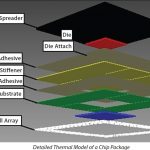
As we move towards packing more and more functionalities and increasing densities of SoCs, the power, thermal and signal integrity issues keep on rising. 3D-IC is a great concept to stack multiple dies on top of each other vertically. While it brings lot of avenues to package dies with multiple functions together, it has challenges… Read More
Predicting Component Temperature Early in Design
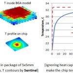
In today’s electronics with multiple functions working together, heat generation is on the rise; sometimes it becomes intolerable. In fact components running at different temperatures can cause timing issues, and very high temperatures can lead to operational issues such as latch-up. An electronic system can contain chips,… Read More
Noise & Reliability of FinFET Designs – Success Stories!
I think by now there has been good level of discussion on FinFET technology at sub-20 nm process nodes and this is an answer to ultra dense, high performance, low power, and billion+ gate SoC designs within the same area. However, it comes with some of the key challenges with respect to power, noise and reliability of the design. A FinFET… Read More
ANSYS Tools Shine at FinFET Nodes!
In the modern semiconductor ecosystem we are seeing rapid advancement in technology breaking past once perceived limits; 28nm, 20nm, 16-14nm, 10nm and we are foreseeing 7nm now. Double and multi-patterning are already being seen along with complex FinFET structures in transistors to gain the ultimate advantages in PPA from… Read More
RedHawk Excels – Customers Endorse
Since a few years, I have been following up Ansys Apachetools for semiconductor design, verification and sign-off. RedHawk is the most prominent platform of tools from Ansys, specifically for Power, Noise and Reliability Sign-off. It has witnessed many open endorsements from several of Ansyscustomers through open presentations,… Read More
Fast & Accurate Thermal Analysis of 3D-ICs
As Moore’s law started saturating on a single semiconductor die, the semiconductor community came up with the approach of growing vertically by stacking dies one above other in a 3D-IC arrangement. However, a major concern with a 3D-IC is that the heat generated by each die can get trapped in the stack, and hence it’s extremely important… Read More


