You are currently viewing SemiWiki as a guest which gives you limited access to the site. To view blog comments and experience other SemiWiki features you must be a registered member. Registration is fast, simple, and absolutely free so please,
join our community today!
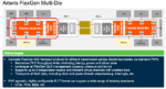
Last year I wrote about Arteris’ introduction of multi-die support for coherent NoCs. This is a very big deal because hyperscalers and OEMs are now building large systems that depend on multi-chiplet architectures and require efficient traffic management between chiplets, in one case as many as 12 compute, fabric/cache and … Read More
Chiplet Summit 2027by Admin on 10-08-2026 at 10:57 pm
All the Solutions for Developing Chiplets
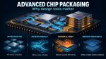
As chipmakers put more computing power into a single system, the challenge extends beyond making individual chips faster. They must connect multiple chips, memory stacks, power supplies, and sometimes optical components in a compact package. In the2026 TSMC OIP Forum talk “Addressing Inter-Die Complexity for 3D Multi-Die… Read More
Vivek Raghuraman is co-founder and CEO of Mixx Technologies. At Intel, he led the first integrated silicon photonics transceiver to commercial release. At Broadcom, Raghuraman took two commercial generations of co-packaged optics through hyperscaler qualification in Meta’s environment. In 2023, together with Rebecca … Read More
Dr. Sunghyun Park earned his B.S. from KAIST and his Ph.D. from MIT’s CSAIL (Computer Science and Artificial Intelligence Laboratory). He built his career across Intel, Samsung Research, and SpaceX as a semiconductor design engineer, before serving as Vice President at Morgan Stanley in New York — a rare combination of… Read More
Analog Bits is expanding its role in advanced semiconductor design with new intellectual property aimed at one of the industry’s most difficult problems: delivering, monitoring, and managing power inside increasingly complex chips.
The company announced that its IP will be included in an upcoming customer test-chip tapeout… Read More
Source: Jonathon Evans and Polychronis Xekalakis, “NVIDIA Vera CPU,” Hot Chips 2026. Performance figures are NVIDIA claims, and several results were based on preproduction or unofficial testing.
NVIDIA’s Vera CPU is a server processor designed specifically for agentic AI, where language models repeatedly observe, reason,… Read More
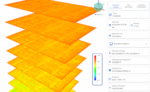
Signoff-quality design tools are mandatory for signoff, though not so good for early design exploration. Signoff demands high accuracy in design description and high precision in analysis. The first requirement can’t be met early in design where architecture decisions are still in flux, and the second depends on very detailed… Read More
How Will You Manage Power, Performance, and Reliability in the Chiplet Era?
Chiplet-based architectures, 2.5D integration, and system-in-package (SiP) designs are unlocking new levels of performance, scalability, and design flexibility. But moving beyond the monolithic SoC also introduces complex interactions among… Read More
The Design Automation Conference in Long Beach was a pleasant surprise. It drew strong attendance from leading companies across the semiconductor ecosystem, along with an impressive number of newcomers. AI-focused EDA companies came out in force—and delivered.
Intel Foundry also made its presence felt, reminding everyone… Read More