*Company Email Required for Registration*
Full-chip SoC debug has become one of the most expensive bottlenecks in modern verification. A single production issue can pull multiple engineers away days as they chase a failure through waveforms, logs, and across hundreds of thousands of lines of code.
In this webinar, we will demonstrate… Read More
ChipEx2026by Admin on 01-22-2026 at 2:46 pm
The major annual event of the Israeli semiconductor industry
ChipEx2026, the largest annual event of the Israeli semiconductor industry, will be held on May 12-13, 2026 in Tel Aviv, Israel. ChipEx2026 showcases companies including manufacturers, developers and suppliers of advanced hardware technologies & services.… Read More
MachineWare, and Andes Technology today announced a collaborative co-emulation solution designed to address the increasing complexity of RISC-V-based chip design. The solution integrates MachineWare’s SIM-V virtual platform, S2C’s Genesis Architect and Prodigy FPGA Prototyping Systems, and Andes’ high-performance… Read More
Faraj Aalaei is a successful visionary entrepreneur with over 40 years of distinguished experience in communications and networking technologies. As a leading entrepreneur in Silicon Valley, Faraj was responsible for building and leading two semiconductor companies through IPOs as a founder and CEO.
Post acquisition of … Read More
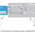
It seems that it has always been that there were packages and ICs, and in the design tool world “never the twain shall meet”. The tools for designing packages were completely separate from the tools used to design IC’s. This was so profoundly true that even after Cadence merged with Valid Logic back in the early 90’s, their Allegro … Read More
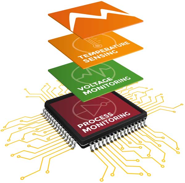
PVT – depending on what field you are in those three letters may mean totally different things. In my undergraduate field of study, chemistry, PVT meant Pressure, Volume & Temperature. Many of you probably remember PV=nRT, the dreaded ideal gas law. However, anybody working in semiconductors knows that PVT stands … Read More
When I hear the company name of ANSYS the first EDA tool category that comes to mind is power noise sign-off. Going to DAC is a great way to find out what’s new with EDA, IP and foundries. There are three places that you can find ANSYS at DAC this year:… Read More
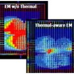
In a world with mobile and IoT devices driven by ultra-low power, high performance and small footprint transistors, FinFET based designs are ideal. FinFETs provide high current drive, low leakage and high device density. However, a FinFET transistor is more exposed to thermal issues, electro migration (EM), and electrostatic… Read More
I think by now there has been good level of discussion on FinFET technology at sub-20 nm process nodes and this is an answer to ultra dense, high performance, low power, and billion+ gate SoC designs within the same area. However, it comes with some of the key challenges with respect to power, noise and reliability of the design. A FinFET… Read More
Since power has become a critical factor in semiconductor chip design, the stress is towards decreasing supply voltage to reduce power consumption. However, the threshold voltage to switch devices cannot go down beyond a certain limit and these results in an extremely narrow margin for noise between the two. And that gets further… Read More