You are currently viewing SemiWiki as a guest which gives you limited access to the site. To view blog comments and experience other SemiWiki features you must be a registered member. Registration is fast, simple, and absolutely free so please,
join our community today!
During my annual holiday meal with one of my favorite EDA icons some rather bold predictions were made. On his side it was more of what he would LIKE to see happen, on my side it was more of what will HAVE to happen for the semiconductor ecosystem to thrive in the coming years.
Mike Gianfagna (Viva Italia!) spent 15+ years with RCA/GE Semiconductor… Read More
I sat down yesterday with Dr. Ajoy Bose, CEO of Atrenta, to get his view of the future of EDA – looking through a high-power “spyglass” of sorts. I first met Ajoy when he was at Software & Technologies. I was then the VP of Engineering for Compass Design Automation and we were considering off-shoring some development. We eventually… Read More
Atrenta did an online survey of their users. Of course Atrenta’s users are not necessarily completely representative of the whole marketplace so it is unclear how the results would generalize for the bigger picture, your mileage may vary. About half the people were design engineers, a quarter CAD engineers and the rest … Read More
Soft IP Qualificationby Paul McLellan on 10-14-2011 at 3:10 pmCategories: EDA
At the TSMC Open Innovation Platform Ecosystem Forum (try saying that three times in a row) next week (on Tuesday 18th), Atrenta will present a paper on the TSMC soft IP qualification flow. It will be presented by Anuj Kumar, senior manager of the customer consulting group.
More and more, chips are not put together what we think of … Read More
If you ask design groups what the biggest challenges are to getting a chip out on time, then the top two are usually verification, and getting closure after physical design. Not just timing closure, but power and area. One of the big drivers of this is predicting and avoiding excessive routing congestion, which is something that … Read More
Fast Track Seminarsby Paul McLellan on 09-15-2011 at 6:11 pmCategories: EDA
Atrenta’s SoC realization seminars, “Fast Track Your SoC Design” have started.The first one was in Ottowa last Tuesday, and it was a full house. In a straw poll, most of the attendees acknowledged facing IP handoff and quality issues. The keynote speaker was Dr Yuejian Wu, director of ASIC development at Infinera… Read More
Atrenta has four seminars coming up on SoC realization. More and more design is actually about finding IP and integrating it together at the block level, and then handing it off to a standard RTL to GDSII flow. The three focus areas are:
- finding quality IP faster
- accelerating IP integration and SoC assembly
- handing off RTL successfully.
…
Read More
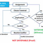
Formal verification has grown in importance as designs have grown and it has become necessary to face up to the theoretical impossibility of using simulation to get complete coverage along with the practical impossibility of simulating enough to even get close.
There are a number of solvers for what is called satisfiability (SAT)… Read More
Design for test at RTLby Paul McLellan on 07-10-2011 at 3:09 pmCategories: EDA
Design for test (DFT) imposes various restrictions on the design so that the test automation tools (automatic test pattern approaches such as scan, as well as built-in self-test approaches) will subsequently be able to generate the test program. For example, different test approaches impose constraints on clock generation… Read More
SOC Realizationby Paul McLellan on 06-27-2011 at 5:28 pmCategories: EDA
There are some very interesting comments to the last entry on SoC Realization and how more and more chips are actually assembled out of IP. There was clearly a lot of discussion in this area at DAC, although most people (Atrenta being an exception) don’t use the term SoC Realization, presumably because it was originated by … Read More


