You are currently viewing SemiWiki as a guest which gives you limited access to the site. To view blog comments and experience other SemiWiki features you must be a registered member. Registration is fast, simple, and absolutely free so please,
join our community today!
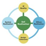
If you just casually peruse most marketing presentations by EDA companies, you’d come to the conclusion most SoCs are designed from scratch, wrestlilng the monster to the ground with bare hands. But the reality is that most SoCs consist of perhaps 90% IP blocks (many of them memories). That still leaves the remaining 10% … Read More
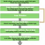
“Power is the new timing” has almost become a cliché. There are a number of reasons for this, not least that increasingly it is power rather than anything else that caps the performance that a given system can deliver. Power is obviously very important in portable applications such as smartphones because it shows through directly… Read More
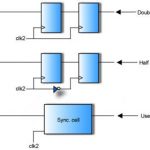
Yesterday I talked to Shaker Sarwary, the senior product director for Atrenta’s clock-domain crossing (CDC) product SpyGlass-CDC. I asked him how it came about. The product was originally started nearly 8 years ago, around the time Atrenta itself got going. Shaker got involved about 5 years ago.
Originally this was a small… Read More
Multiple, independent clocks are quintessential in SoCs and other complex ASICs today. In some cases, such as in large communications processors, clock domains may number in the hundreds. Clock domain crossings pose a growing challenge to chip designers, and constitute a major source of design errors–errors that can… Read More
"Managing increasing complexity through higher-level of abstraction: What the past has taught us about the future" Dr. Ajoy Bose, Atrenta CEO
Here is the abstract:
Time to market and design complexity challenges are well-known; we have all seen the statistics and predictions. A well-defined strategy to address … Read More
Atrenta Inc., the leading provider of Early Design Closure® solutions to radically improve design efficiency throughout the IC design flow, announced today that it will participate in a worldwide social media platform aimed at facilitating mass communication for electronic design professionals through Web 2.0 technologies.… Read More
My vote for most compelling technology at #47DAC is 3D technology. No, I don’t mean Hollywood-style 3D, I’m talking about vertical stacked-die system on chip design. This design approach basically means putting different parts of the system on different silicon substrates, so you can use the right technology for each part, and… Read More