Last week I presented at the 3D ASIP EDA Tutorial and attended the Conference. In previous years, leading edge papers were presented from large companies pushing a solution to meet their needs. These companies had the resources and clout to achieve some astounding successes, but the lingering question was: “what other product… Read More

Tag: 3d-ic
Boost the Market for Interposer and 3D ICs with Assembly Design Kits

The traditional system-on-chip (SoC) design process has fully qualified verification methods embodied in the form of process design kits (PDKs). Why is it that chip design companies and assembly houses have no IC/package co-design sign-off verification process?
Package die are often produced using multiple processes and… Read More
Will 3DIC Ever Be Cheap Enough for High Volume Products?
More news from the 3DASIP conference. Chet Palesko of SavanSys Solution had an interesting presentation with the same title as this blog (although this blog draws from several other presentations too). Chet took a look at what aspects of 3D are likely to get cheaper going forward. He took as a starting point that stuff that is not … Read More
3D, The State of the State
I have been at the 3D ASIP conference that is held every year in Burlingame. It is far and away the best place to get a snapshot on what is going on in 3D (and 2.5D) IC design each year. One of the presentations was by the guys from Yole on where the industry is right now. Other presentations were on pathfinding, power reduction (did you know… Read More
3DIC in Burlingame
Every year in December is what I think of as the main 3D IC conference where you can get up to speed on all the latest. Officially it is called 3D Architectures for Semiconductor and Packaging or 3D ASIP. It is held in the Hyatt Regency in Burlingame (the one right by 101 near the airport). This year it is from December 10-12th.
The first… Read More
Solution for PI, TI & SI Issues in 3D-ICs
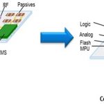
As we move towards packing more and more functionalities and increasing densities of SoCs, the power, thermal and signal integrity issues keep on rising. 3D-IC is a great concept to stack multiple dies on top of each other vertically. While it brings lot of avenues to package dies with multiple functions together, it has challenges… Read More
Noise & Reliability of FinFET Designs – Success Stories!
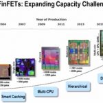
I think by now there has been good level of discussion on FinFET technology at sub-20 nm process nodes and this is an answer to ultra dense, high performance, low power, and billion+ gate SoC designs within the same area. However, it comes with some of the key challenges with respect to power, noise and reliability of the design. A FinFET… Read More
ANSYS Tools Shine at FinFET Nodes!
In the modern semiconductor ecosystem we are seeing rapid advancement in technology breaking past once perceived limits; 28nm, 20nm, 16-14nm, 10nm and we are foreseeing 7nm now. Double and multi-patterning are already being seen along with complex FinFET structures in transistors to gain the ultimate advantages in PPA from… Read More
The Intel Resurgence?
There is an interesting article on Seeking Alpha about Intel. Interesting because it is written by someone with both fabless semiconductor experience and a talent for strategic thinking. It’s a good read and like most Seeking Aplha semiconductor articles the comments are hilarious. Give the guy a penny and click over HERE, he … Read More
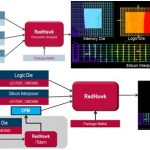
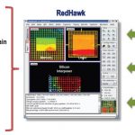
RedHawk Excels – Customers Endorse
Since a few years, I have been following up Ansys Apachetools for semiconductor design, verification and sign-off. RedHawk is the most prominent platform of tools from Ansys, specifically for Power, Noise and Reliability Sign-off. It has witnessed many open endorsements from several of Ansyscustomers through open presentations,… Read More