What’s new at Cadence? Quite a bit actually. I have always been a Cadence fan, I mean really, they gave birth to modern EDA. Unfortunately, Cadence really lost me during the Avant! legal action, the Mike Fister years, and EDA360. Recently, however, Cadence has made some big changes that will definitely get them back on my good side.… Read More
Tag: 20nm
Sagantec Update: More EDA Consolidation!
Adding sophisticated 2D dynamic compaction technology to address 20nm and 14nm challenges. Santa Clara, California – May 3 ,2012 – Sagantec today announced that it has acquired Dutch startup NP-Komplete Technologies BV (Eindhoven, The Netherlands) for its physical design compaction and migration solutions based on a sophisticated… Read More
20nm IC Design at IBM using Cadence Tools
Collaboration between EDA, Foundry and Design was the key idea today in a webinar hosted by IBM and Cadence about 20nm custom IC design. The three presenters were:
John Stabenow, Cadence
Jeremiah Cessna, Cadence
Keith Barkley, IBM… Read More
IC design at 20nm with TSMC and Synopsys
While the debate rages on about 28nm yield at foundry juggernaut TSMC, on Monday I attended a webinar on 20nm IC design hosted by TSMC and Synopsys. Double Patterning Technology (DPT) becomes a requirement for several layers of your 20nm IC design which then impact many of your EDA tools and methodology.… Read More
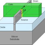
Next Generation Transistors
We have all heard that planar transistors have run out of steam. There are two ways forward. The one that has garnered all the attention is Intel’s trigate which is their name for FinFET. The other is using thin film SoI which ST is doing. TSMC and Global seem to be going the FinFET way too, although at a more leisurely pace. But … Read More
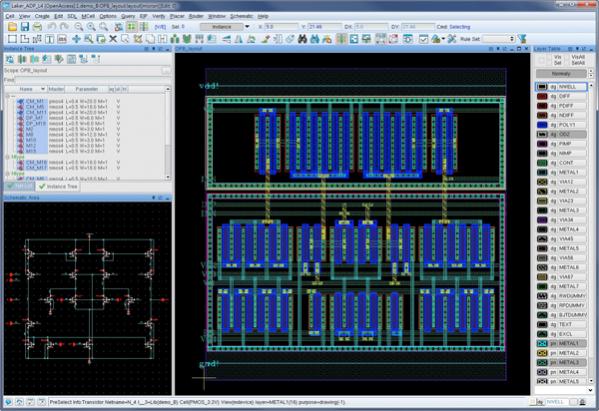
Laker Wobegon, where all the layout is above average
TSMC’s technnology symposium seems to be the new time to make product announcements, with ARM and Atrenta yesterday and Springsoft today.
There is a new incarnation of Springsoft’s Laker layout family, Laker[SUP]3[/SUP] (pronounced three, not cubed). The original version ran on its own proprietary database.… Read More
Analog Automation – Needs Design Perspective
Recently I was researching the keynote speeches of isQED (International Society for Quality Electronic Design) Symposium 2012 and saw the very first, great presentation, “Taming the Challenges in Advanced Node Design” by Tom Beckley, Sr. VP at Cadence. I know Tom very well as I have worked with him and I admire his knowledge, authority… Read More
Semiconductors: A Decade of Invention… A World of Solutions
Please join IBM, Samsung Electronics, Co., Ltd., and GLOBALFOUNDRIES at the 2012 Common Platform Technology Forum. The forum will showcase the alliance’s technological progress and how joint collaboration and innovation is setting the direction for industry-leading solutions to enable next-generation products. … Read More
Layout for analog/mixed-signal nanometer ICs
Analog has always been difficult, a bit of a black art persuading a digital process to create well-behaved analog circuits, capacitors, resistors and all the rest. In the distant past, we would solve this by putting the analog on a separate chip, often in a non-leading-edge process. But modern SoCs integrate large amounts of digital… Read More
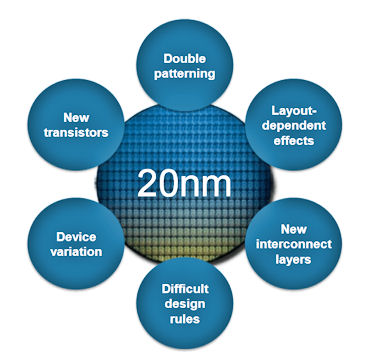
20nm SoC Design
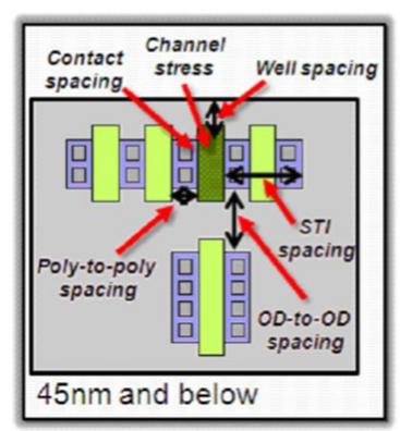
There are a large number of challenges at 20nm that didn’t exist at 45nm or even 32nm.
The biggest issues are in the lithography area. Until now it has been possible to make a reticle using advanced reticle enhacement technology (RET) decoration and have it print. Amazing when you think that at 45nm we are making 45nm features… Read More


