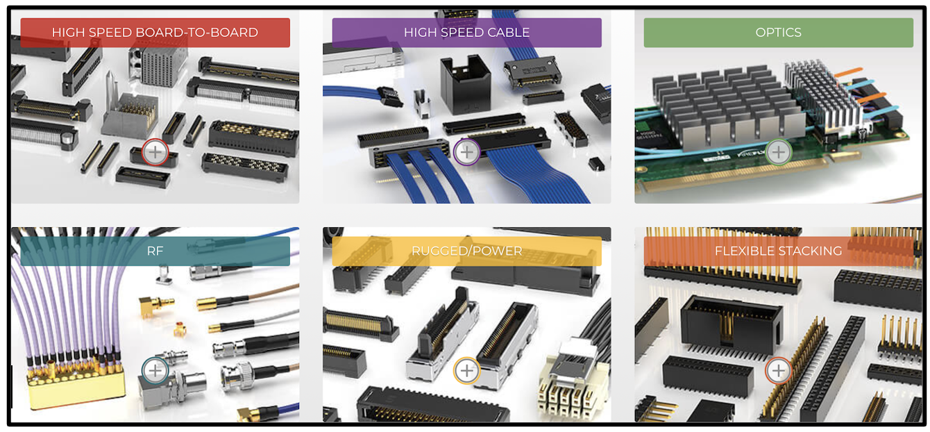
If you’ve spent a lot of time in the chip or EDA business, “design” typically means chip design. These days it means heterogeneous multi-chip design. If you’ve spent time developing end products, “design” has a much broader meaning. Chips, subsystems, chassis and product packaging are in focus. This is just a short list if you consider all the aspects of system design and its many disciplines, both hardware and software. Samtec lives in the system design world. The company helps connect the chiplets, chips, subsystems and racks that comprise a complete system.
There is a huge array of products from Samtec that need to be considered in any system design project. The screenshot above gives you a sense of the diversity involved. Choosing a particular connector will impact other choices. Not all combinations of Samtec products are viable as an integrated solution. The company has developed tools to help system designers navigate all this. Last year, I described something called Solution Blocks that assisted with choices that were compatible. Samtec has now taken that concept to the next level by adding visualization, along with more control and a broader perspective. If the entire semiconductor ecosystem worked this way, design would be a lot easier. Let’s take a short tour of visualizing system design with Samtec’s Picture Search.
Seeing is Believing
A link is coming so you can try this out for yourself. Here are a couple of examples of what’s possible. We’ll start with one of the many edge connectors available from Samtec. I chose the vertical Edge Rate® High-Speed Edge Card Connector. The initial configuration is shown below, including a high-resolution image that can be rotated for different views.
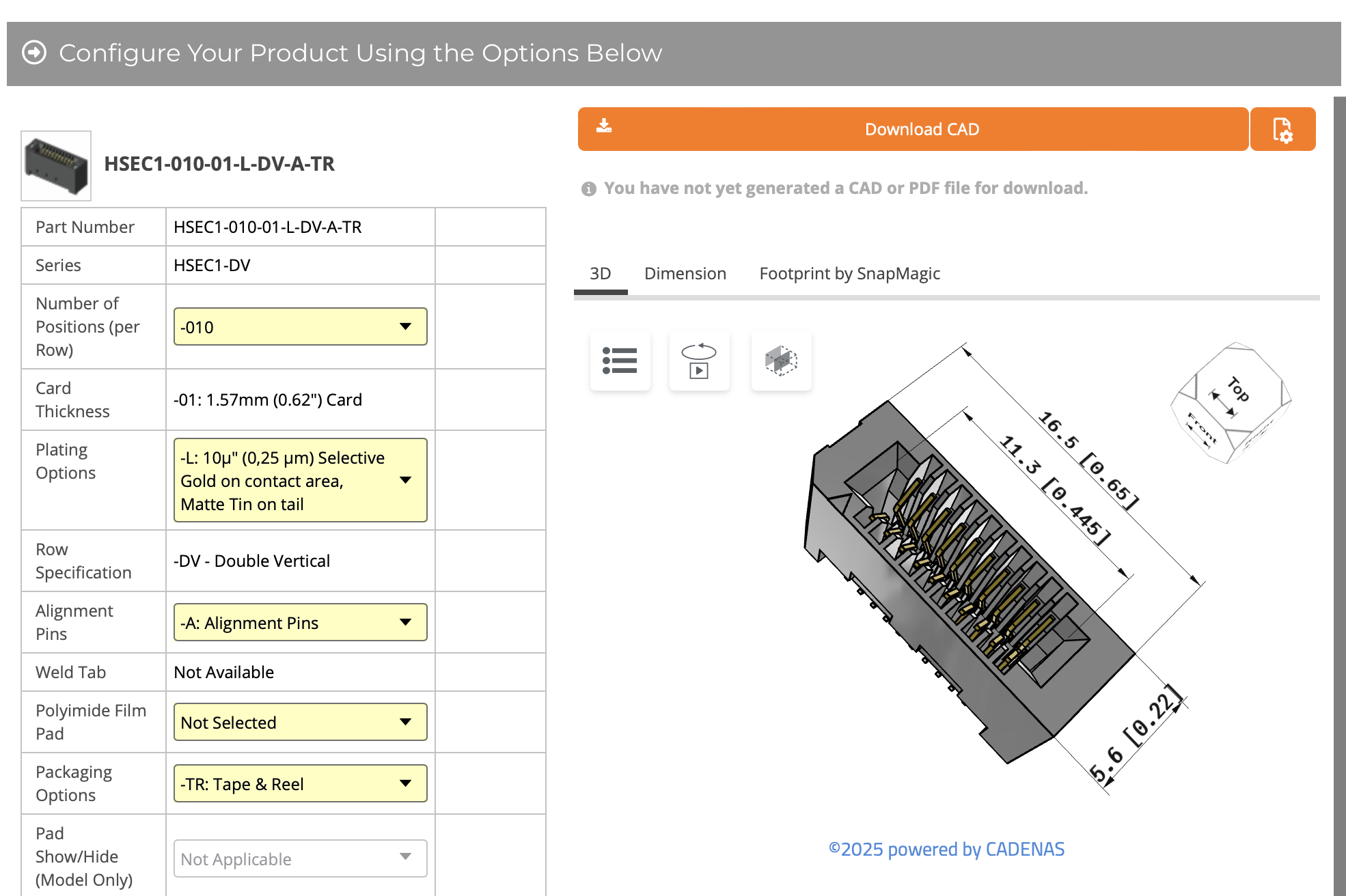
I decided to change the number of positions per row from 10 to 50. I also specified a polyimide file pad. In seconds, I got an updated image with detailed dimensions, see below.
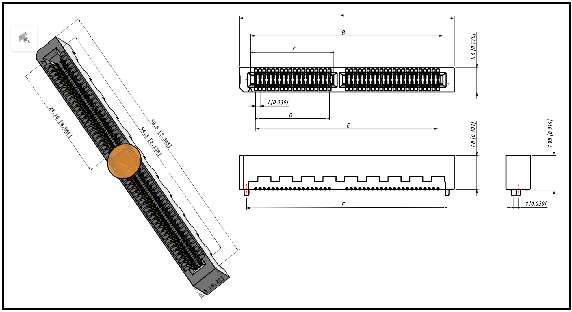
The system summarized the features as shown below, along with detail specs, volume pricing/availability and extensive compliance data.
- Optional weld tab for mechanical strength
- 00 mm pitch, up to 140 positions
- Accepts .062″ (1.60 mm) thick cards
- Current rating: 2.2 A max
-
Voltage rating: 215 VAC/304 VDC max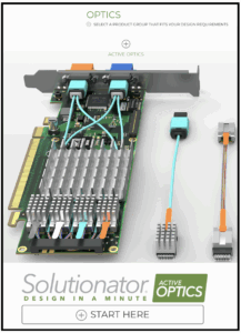
This all took seconds to do. The ability to perform what-if experiments to converge on the best solution is certainly enabled by a system like this.
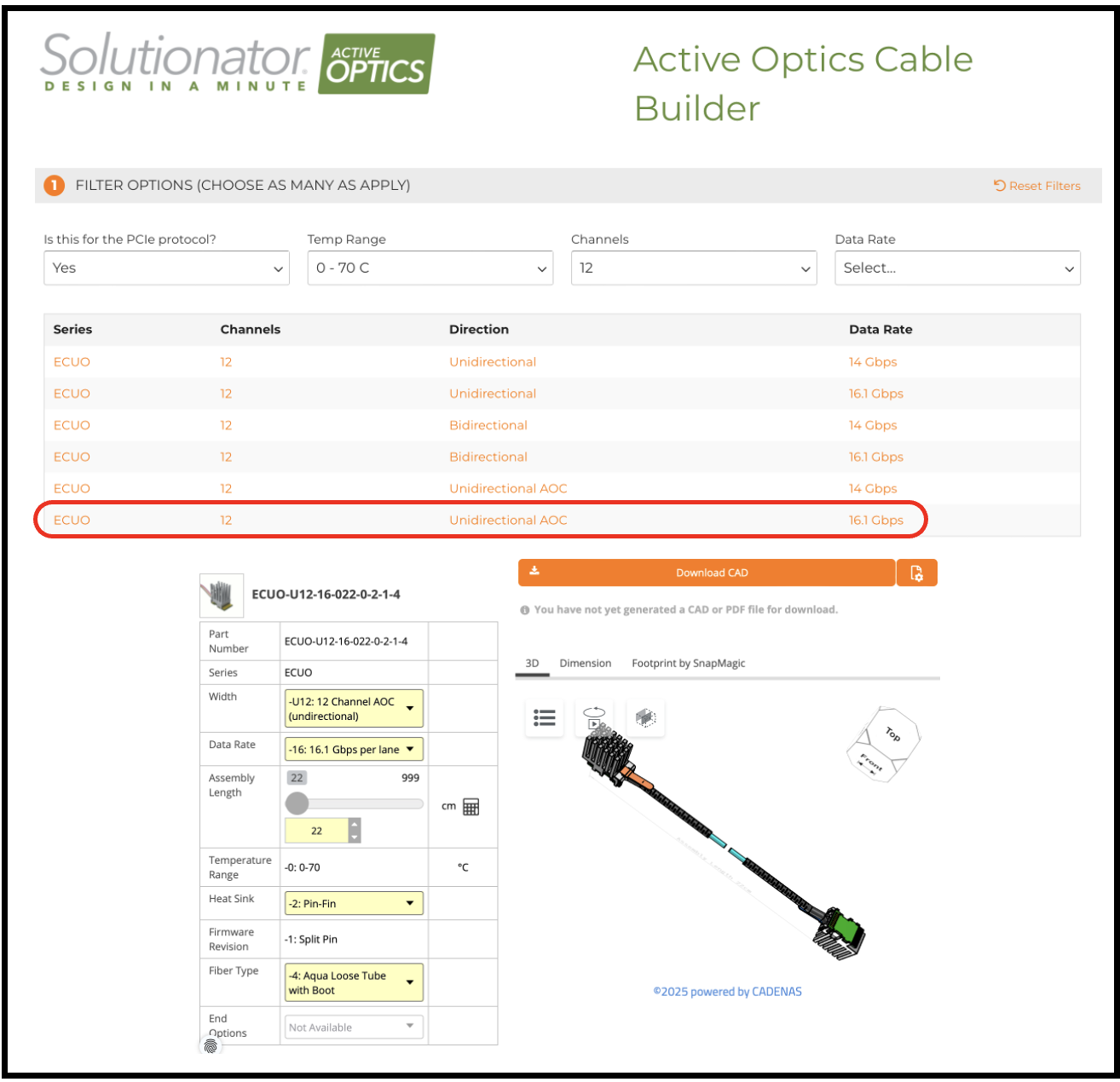
For one more experiment, I decided to try the Solutionator instead of browsing categories. Here, I chose active optics. I then invoked the Solutionator interface for Active Optics, with its promise to “design in a minute.”
With the Active Optics Cable Builder interface, I could quickly browse the various options available. I chose a 12-channel, 16.1 Gbps, unidirectional AOC and instantly received the 3D diagram and all the specs as before. See below.
I could go on with more examples of how this new technology from Samtec makes it easier to pick the right components to implement your next system. The communication, latency and power requirements for advanced semiconductor systems continues to get more demanding. The technology delivered by Samtec is a key ingredient to developing channels that meet all those requirements. And the process just got easier with Samtec’s picture search.
To Learn More
If high performance channels matter to you, you must try this new technology from Samtec. If power, performance and form factor are key care abouts, you must try it as well. You can access the starting point for your journey here. Have fun visualizing system design with Samtec’s Picture Search.
Share this post via:


Comments
There are no comments yet.
You must register or log in to view/post comments.