There are many unsung heroes in our industry – companies that provide unique services and expertise that enable the rapid advances in fabrication process development that we’ve come to rely upon. Some of these companies offer “back-end” services, assisting semiconductor fabs with yield diagnostic engineering and failure analysis. Some are “front-end” companies that pursue advanced research into promising new materials and processing techniques, and then assist with technology transfer to production manufacturing. We tend to focus on the large semiconductor foundries and their process roadmaps, yet the underlying support from these engineering firms is fundamental to the industry as a whole.
An exemplary front-end services company is Intermolecular, the Silicon Valley science hub of the EMD Electronics. They offer process development research and characterization services, spanning a wide range of materials – e.g., metal alloys, oxides/nitrides, thin films for specialized applications.
With each new process node, extensive investigations into new materials are pursued, to determine the optimum stoichiometry and electrical properties. This is especially evident in the pursuit of alternative memory technologies. A specific example is the introduction of new ferroelectric materials for very high density, non-volatile data storage.
Background
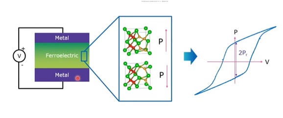
A ferroelectric material is a special dielectric, in that it exhibits two (stable) remanent polarization states. The figure below illustrates the hysteresis curve of the crystalline polarization when an applied voltage is cycled across the dielectric – note the two intersections of the curve with the vertical axis when the applied voltage is zero, representing the stored “state” of the material.

The polarization is the contribution of the electric dipoles in the material to the electric flux between the terminals in the presence of an electric field. The formula for the dielectric constant in the material is: epsilon = (epsilon_0 + P/E), where epsilon_0 is the dielectric constant of free space, P is the polarization in the material, and E is the applied field. The curve for a conventional, non-ferroelectric material would be a straight line through the origin – i.e., no polarization when the applied voltage is removed.
Note in the figure that the chemical bond orientation in the material differs slightly in the two states, resulting in the remanent polarization.
(The term ferroelectric is a bit misleading – there is no iron (Fe) constituent in the dielectric material. The hysteresis curve of the dielectric polarization resembles the curve of a ferromagnetic material in the presence of an applied magnetic field. After the external field is removed, the ferromagnetic material retains a magnetic polarization. When the concept of remanent electrical polarization in a dielectric was first demonstrated, the term ferroelectricity was introduced, which has lasted.)
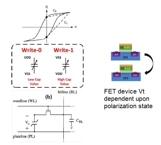
The two polarization states of the ferroelectric material suggest that it may be used as part of a memory bit circuit implementation. The figure below illustrates a couple of potential implementations:

One depicts the ferroelectric material as a replacement for the storage capacitor in a 1T1C bitcell. Unlike a conventional DRAM, note that no refresh of storage charge due to leakage current is required – data storage is represented by a dielectric polarization state, not by the amount of charge stored on the bitcell capacitance. The other implementation depicted above shows the ferroelectric material directly integrated in the dielectric gate stack of a field-effect transistor. The two polarization states of the material will result in different threshold voltages for the device, representing the stored data value.
As you might imagine, the crystalline properties of the dielectric material are crucial to the magnitude of the polarization states and the opening of the hysteresis curve.
Intermolecular Webinar on Ferroelectric Materials Optimization
I had an opportunity to view an outstanding webinar from Intermolecular, describing their recent investigations into ferroelectric materials. Their prototype fab capabilities provided atomic level deposition (ALD) of a variety of hafnium oxide (HfO2) and zirconium oxide (ZrO2) films.
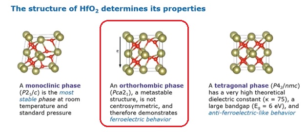
An image from the webinar is shown below, for the case of HfO2. There are three crystalline topologies for these oxides, however only one demonstrates attractive ferroelectric behavior.

It is therefore necessary to ensure the process flow for depositing (and crystallizing) the film results in a very high percentage of material with the desired crystalline structure.
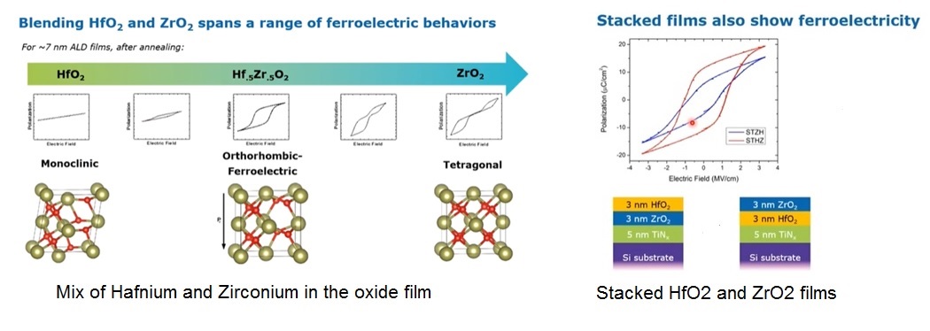
Another process experiment pursued by the Intermolecular team evaluated the ferroelectric properties of a stoichiometric mix of hafnium and zirconium in the dielectric in a single thin film, as well as stacking separate ALD-deposited HfO2 and ZrO2 layers.

Even if you’re not directly involved in advanced process development, I would encourage you to view this webinar presentation from Vijay Narasimhan at Intermolecular. It is extremely informative, starting with the basics of ferroelectricity, and offering insights into the R&D flow for materials evaluation – e.g., deposition/annealing, crystalline spectroscopy, and electrical characterization.
Here is the webinar replay link.
Here is a link to more information on the front-end services provided by Intermolecular.
Also Read:
Executive Interview: Casper van Oosten of Intermolecular, Inc.
Integrating Materials Solutions with Alex Yoon of Intermolecular
Ferroelectric Hafnia-based Materials for Neuromorphic ICs
Share this post via:


Musk’s Orbital Compute Vision: TERAFAB and the End of the Terrestrial Data Center