
In the relentless race to power next-generation artificial intelligence (AI) systems, data connectivity has emerged as the critical bottleneck. As AI models balloon in size—from billions to trillions of parameters—compute resources alone are insufficient. According to Ayar Labs, approximately 70% of AI compute time is wasted waiting for data, a inefficiency that escalates exponentially with system scale. Traditional copper-based electrical I/O, while reliable for intra-rack connections, falters under the demands of multi-rack AI clusters. Power consumption soars, latency spikes, and bandwidth caps out, rendering electrical solutions obsolete for hyperscale datacenters. Enter the strategic collaboration between Alchip Technologies and Ayar Labs, unveiled in September 2025, which promises to shatter these barriers through co-packaged optics (CPO) and advanced packaging innovations.

At the TSMC North America Open Innovation Platform (OIP) Ecosystem Forum on September 26, the partnership fuses Alchip’s expertise in high-performance ASIC design and 2.5D/3D packaging with Ayar Labs’ pioneering optical I/O chiplets. This isn’t mere integration; it’s a holistic ecosystem leveraging TSMC’s COUPE (Co-packaged Optics with Unified Packaging and Electronics) technology to embed optical engines directly onto AI accelerator packages. The result? A reference design platform that enables seamless, multi-rack scale-up networks, transforming AI infrastructure from rigid, power-hungry monoliths into flexible, composable architectures.
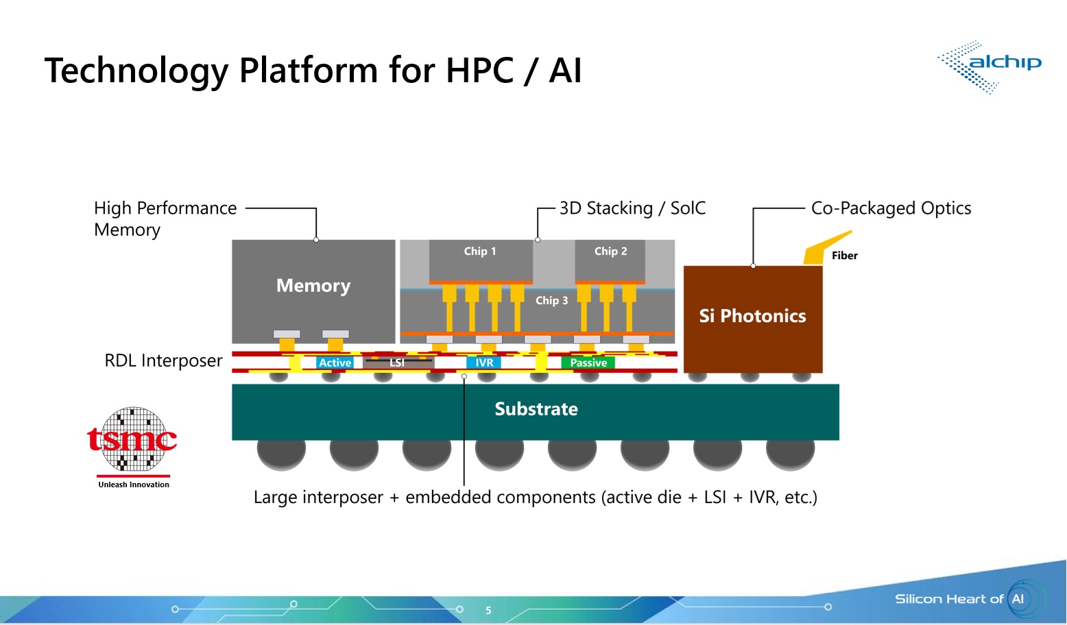
At the heart of this solution lies Ayar Labs’ TeraPHY™ optical engines, silicon photonics-based chiplets that replace cumbersome pluggable optics with in-package optical I/O. Each TeraPHY engine employs a stacked Electronic Integrated Circuit (EIC) and Photonic Integrated Circuit (PIC) architecture, utilizing microring modulators for dense, efficient light-based data transmission. The EIC, fabricated on advanced nodes, handles protocol-specific features like UCIe-A (Universal Chiplet Interconnect Express-Advanced) for logic protocols such as CHI, while the PIC manages optical signaling. A detachable optical connector simplifies manufacturing, assembly, and testing, ensuring high-volume scalability. Protocol-agnostic by design, TeraPHY supports endpoints like UALink, PCIe, and Ethernet, with forward error correction (FEC) and retimer logic delivering raw bit error rates below 10^-6 for PAM4 CWDM optics—achieving single-hop latencies of 100-200 nanoseconds. Future DWDM variants promise even lower 20-30 ns latencies and BERs under 10^-12.
Alchip complements this with its I/O protocol converter chiplets, bridging UCIe-A (streaming mode) to scale-up protocols, and integrated passive devices (IPDs) that optimize signal integrity through custom capacitors. Their prototype, showcased at Booth 319 in Taipei and Silicon Valley, integrates two full-reticle AI accelerators, four protocol converters, eight TeraPHY engines, and eight HBM stacks on a common substrate. This configuration unlocks over 100 Tbps of scale-up bandwidth per accelerator and more than 256 optical ports, dwarfing electrical I/O’s limits. Power density remains manageable, as optics reduce end-to-end energy per bit by minimizing electrical trace lengths and avoiding the thermal overhead of pluggables.
The implications for AI workloads are profound. In scale-up networks, where XPUs (AI processing units) must act as unified entities—scaling from 100 to 1,000 units—the joint solution enables XPU-to-XPU, XPU-to-switch, and switch-to-switch connectivity with path diversity for ultra-low latency. Extended memory hierarchies, pooling DRAM across racks via optical links, boost application metrics like training throughput by 2-3x, per preliminary simulations. Energy efficiency improves dramatically: Optical I/O consumes up to 10x less power than copper equivalents, critical as AI racks approach 100kW densities. For hyperscalers like those deploying GPT-scale models, this means greener, more interactive datacenters capable of real-time inference at exascale.
This collaboration underscores a broader industry shift toward disaggregated, photonics-driven computing. By addressing reach limitations beyond copper’s 1-2 meter horizon and enhancing radix for massive parallelism, Alchip and Ayar Labs are not just solving today’s challenges but future-proofing AI. As Vladimir Stojanovic, Ayar Labs’ CTO and co-founder, notes, “AI has reached an inflection point where traditional interconnects limit performance, power, and scalability.” Erez Shaizaf, Alchip’s CTO, echoes this, emphasizing the need for “innovative, collaborative advanced packaging.” With production-ready test programs and reliability qualifications, the duo is poised to accelerate adoption, potentially slashing AI deployment costs by 30-50% through efficiency gains.
Bottom line: This partnership heralds a new era of AI infrastructure: scalable, flexible, and composable. As models grow unabated, optical CPO will be indispensable, and Alchip-Ayar Labs’ blueprint offers a proven path forward. Hyperscalers take note—this is the optics revolution AI has been waiting for.
Also Read:
Alchip’s 3DIC Test Chip: A Leap Forward for AI and HPC Innovation
Alchip Launches 2nm Design Platform for HPC and AI ASICs, Eyes TSMC N2 and A16 Roadmap
Alchip’s Technology and Global Talent Strategy Deliver Record Growth
Share this post via:


Comments
There are no comments yet.
You must register or log in to view/post comments.