
During my most recent Taiwan trip I was not only afforded a meeting with Dr Mark Liu, Sr VP of TSMC, a guided tour of GigaFab #12 was also included. Even more impressive, I’m now considered “Elite” by Eva Airlines so I automatically get the good seats, better food, and VIP service. My wife, however, is not impressed with my Elite status so I still have to do chores around the house.

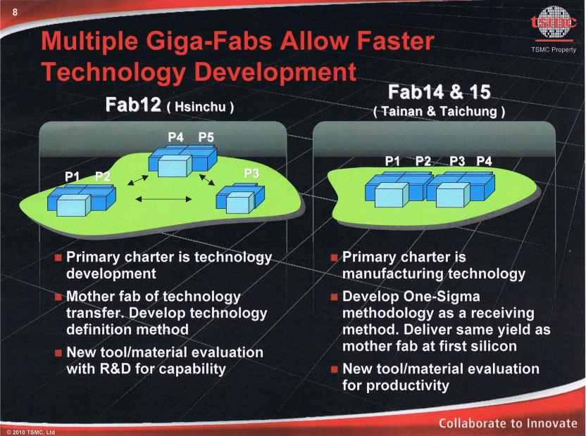
Mark Liu ramped up TSMC’s first 200mm fab in 1993 and has been building fabs for TSMC ever since. Mark’s favorite topic is the 300mm GigaFabs, Fab#12, Fab#14, and Fab #15 which TSMC just broke ground on last month. Clearly TSMC has learned a valuable lesson from the 40nm wafer shortage experience. Not having enough capacity is far more costly than having too much. After 40nm, customer priorities have certainly changed: Capacity is now the 1st concern with price a close 2[SUP]nd[/SUP], and last but not least design enablement. Please note that the perceived value of semiconductor design enablement is often overlooked but it is clearly the key enabler to TSMC’s expansive customer base.
After putting on the clean room space suit and being lightly air washed I entered a GigaFab for the first time and was literally speechless. If you know me personally, being speechless is not one of my strong suits so this was a new experience.
The insignias on the machines were logos and acronyms that I recognized but what struck me was the total automation of a GigaFab. Machines outnumbered man exponentially with 99% automation. Shuttles zoomed around on tracks above delivering thousands of 40nm wafers to the 300+ steps in the semiconductor manufacturing process. The few people I did see were at monitoring stations. Even more impressive than the billions of dollars of hardware in a GigaFab, is the millions of lines of software developed to run it: Automated Material Handling Systems (AMHS) for transporting, storing, and managing semiconductor wafer carriers and reticles plus Manufacturing Execution Systems (MES) software to manage overall production efficiency.
This year TSMC will spend a record $5.9B on capital expenditures. Approximately 75% will be used to expand TSMC’s 65/40/28nm technology capacity and 15% will be used for mainstream processes. The remainder will be used for equipment, R&D expenses, and new business such as solar and LED. TSMC’s newest Gigafab, Fab 15, will cost an estimated $9.4B. TSMC is also set to complete Phase 5 expansion at Fab 12, and Phase 4 expansion at Fab 14.
According to the most recent management report, TSMC has accelerated its capacity expansion plan for 2010. Total managed capacity was 2,749K 8-inch equivalent wafers in 2Q10, increased by 7% from 2,566K in 1Q10. Current capacity plan calls for an overall increase by 14% to 11,299 8- inch equivalent wafers, compared with 11,247 8-inch equivalent wafers planned in the last quarter.
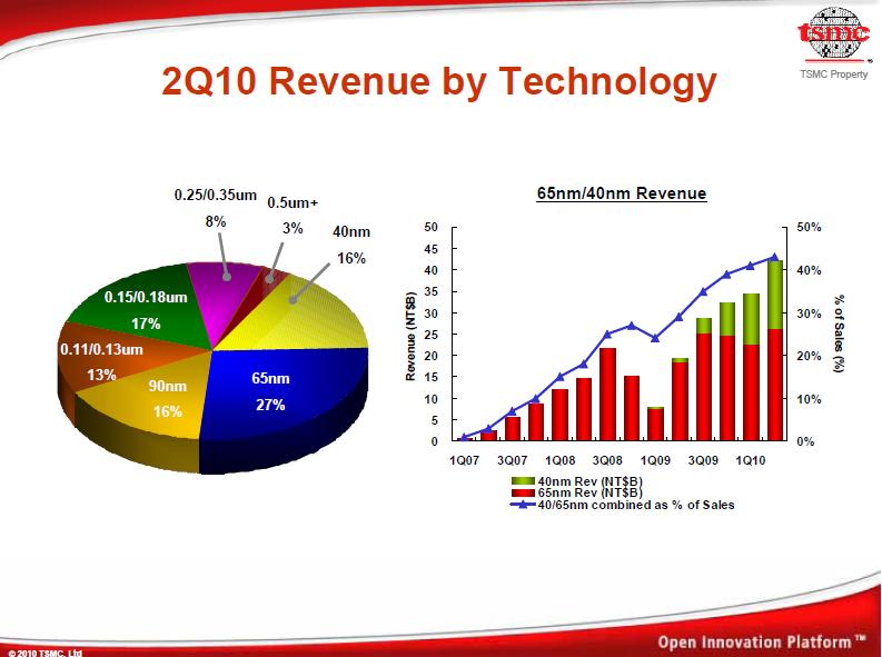
Demand for TSMC’s advanced technology wafers in all major semiconductor market segments again increased quarter to quarter. Among the advanced technologies, 40nm not only increased an additional 2% of TSMC’s revenue share, the output of Gigafab wafers processed using 40nm technology increased by 30% sequentially.
The 40nm race is officially over, TSMC wins by a landslide in regards to capacity, price, and design enablement. The race for 28nm dominance however is still on between TSMC, Samsung, and GlobalFoundries. Samsung is in production at 32nm so moving to 28nm should just be a process shrink. For TSMC and GlobalFoundries, 28nm is a completely new node which will bring new technical challenges. Still, in my opinion, the foundry race to 28nm is too close to call today and it will certainly be an exciting finish!
Share this post via:


Comments
There are no comments yet.
You must register or log in to view/post comments.