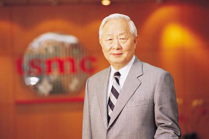
 Given the compressed time between 20nm and 16nm, twelve months versus the industry average twenty four months, it is time to start talking about 10nm, absolutely. Next Tuesday is the 19th annual TSMC Technology Symposium keynoted of course by the Chairman, Dr. Morris Chang.
Join the 2013 TSMC Technology Symposium. Get the latest on:
- TSMC’s 20nm, 16nm, and below process development status including FinFet and advanced lithography insights
- TSMC’s new High-Speed Computing, Mobile Communications, and Connectivity & Storage technology development
- TSMC’s robust Specialty Technology portfolio that includes CMOS Image Sensor (CIS), Embedded Flash, Power IC and MEMS
- TSMC’s GIGAFAB™ programs and improvements that enhance time-to-volume
- TSMC’s 18-inch manufacturing technology development
- TSMC’s Advanced Backend Technology for 3D-IC, CoWoS (Chip-on-Wafer-on-Substrate), and BOT (Bump-on-Trace)
- New Design Enablement Flows and Design Services on TSMC’s Open Innovation Platform®
TSMC takes this opportunity each year to let customers know what is coming and get feedback on some of the challenges we will face in the coming process technologies. I remember 2 years ago when TSMC asked customers openly if they were ready for FinFETs. The answer was mixed, the mobile folks definitely said yes but the high performance people were not as excited. Here we are, two years later, with FinFET test chips taping out. So yes, these conferences are important. This is the purest form of collaboration and SemiWiki is happy to be part of it.
TSMC will also let us know that 20nm is not just on schedule but EARLY. They have been working around the clock to make sure our iPhone6s arrive on time so don’t expect any 20nm delays. In fact, recent news out of Hsinhcu says TSMC will begin installing 20nm production equipment in Fab 14 two months early of the June 2013 target. 20nm is also the metal fabric for 16nm FinFETs so expect no delays there either.
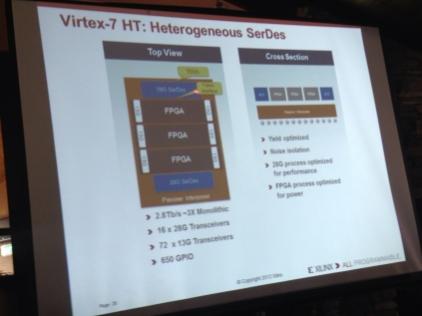
The COWOS update will be interesting. Liam Madden, Xilinx Vice President of FPGA development, did the keynote at the International Symposium on Physical Systems (ISPD) last month and three-dimensional integration was the focus on the kickoff day. EETimes did a nice write up on it: 3-D Integration Takes Spotlight at ISPD:
“For many years, designers kept digital-logic, -memory and analog functions on separate chips—each taking advantage of different process technologies,” said Madden. “On the other side are system-on-chip [SoC]solutions, which integrate all three functions on the same die. However now there is a third alternative that takes advantage of both worlds—namely 3-D stacking.”

3D transistors plus 3D IC integration will keep the fabless semiconductor moving forward at a rapid pace. If you would like to learn more, Ivo Bolsens, CTO of Xilinx, will be keynoting the Electronic Design Processing Symposium in Monterey, CA this month. The abstract of his keynote is HERE.
There is also a 3D IC panel “Are we there yet?” moderated by Mr 3D IC himself Herb Reiter. Herb will be joined by Dusan Petranovic of Mentor Graphics, Brandon Wang of Cadence, Mike Black of Micron, and Gene Jakubowski of E-System Design. Abstracts are HERE. Register today, room is limited!
Share this post via:


Comments
There are no comments yet.
You must register or log in to view/post comments.