TSMC versus Global Foundries Part II

TSMC versus Global Foundries Part II
by Daniel Nenni on 01-17-2010 at 11:52 am

The foundry business is a tough one. The golden age of semiconductors is clearly over and what remains is a highly competitive marketplace. This blog follows up my original TSMC vs Global Foundries which is the single most viewed page on my site.

Case in point #1: Founded in 2000, SMIC Semiconductor Manufacturing International Corporation is billed as one of the leading semiconductor foundries in the world and the largest and most advanced foundry in Mainland China. Harvard Business School even wrote a case study on SMIC’s business model, characterized as a Reverse Build-Operate-Transfer (BOT). Unfortunately cheap labor does not a foundry make. It takes highly experienced workers, advanced manufacturing technology, strategic marketing, and an ultra competitive business model. The semiconductor foundry business is a marathon, not a sprint. Also see TSMC vs SMIC.

Case in point #2: Chartered Semiconductor was created in 1987 as one of the world’s dedicated semiconductor foundries. Chartered Semiconductor continued a string of losing quarters until the Abu Dhabi government-owned Advanced Technology Investment Company (ATIC) acquisition was passed by investors in a majority vote. Shareholders bought Chartered shares at the 1999 initial public offering (IPO) price of S$3.34, the shares were later consolidated at 10 for 1, so they effectively cost S$33.40 each. ATIC paid S$2.68 a share. Chartered had experienced workers and strategic marketing (Common Platform), but lacked the advanced manufacturing technology and competitive business model to be successful.
2010 brings us a truly global foundry with the ATIC acquisitions of the manufacturing arm of AMD and Chartered Semiconductor. Global Foundries now employs 10,000+ people spanning 3 continents and 12 locations with manufacturing operations in Singapore, Dresden, Germany, and a new leading-edge fab under construction in Saratoga County, New York. Global Foundries was founded with $4.5 billion in cash, with future backing going up to $7B. The New York fab alone will cost an estimated $4.5B.

GFI now has about $3B in revenues from more than 150 customers that include many of the world’s top fabless and fab-lite companies, such as AMD, Qualcomm, STMicro, IBM, and Toshiba. Process geometries in production are: .5um, .35um, .25um, .13um, .18um, 90nm, 65nm, and 45/40nm. Process geometries in planning are: 32/28nm and 22/20nm. Planned capacity is 1.6 million 300mm wafers annually by 2014, supplemented by 2.2 million 200mm wafers a year. Global Foundries has highly experienced workers from Chartered Semiconductor and AMD, cutting edge manufacturing technology from AMD and IBM, strategic marketing from Common Platform, add in a competitive business model and you will have the #2 foundry in the world.

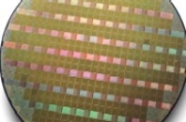
In comparison TSMC has 23,000+ employees and will add 3,000 more in 2010. With $10B+ in annual revenues, TSMC accounts for 50% of the foundry market revenue and 80% of the profits. TSMC is considered a first source for semiconductor manufacture, meaning that leading fabless semiconductor companies work with TSMC first, then replicate manufacturing at the other foundries for redundancy and cost reductions. Global Foundries will challenge TSMC for first sourcing with AMD manufacturing technology and a manufacturing process partnership with IBM. In fact the first production 28nm wafers by a foundry were displayed by GFI at the Consumer Electronics show in Las Vegas this month. At least one of the wafers contained AMD/ATI GPUs.

Unfortunately the semiconductor foundry market is a maturing industry and likely to experience single digit annual growth in coming years. To diversify, TSMC is investing heavily in solar power and light-emitting diodes. Both are fast growing markets, have technological overlap with chip production, and offer far better margins and upside potential. There is a reason why TSMC is the #1 foundry in the world and I don’t see that changing anytime soon. But competition breeds innovation so the foundry business will be much more interesting to watch with GFI challenging TSMC.


TSMC Yields @ 28nm!

TSMC Yields @ 28nm!
by Daniel Nenni on 12-31-2009 at 8:00 pm


It was an interesting week in Taiwan for sure. Typhoon Fanapi, lightning storms, the first 28nm production silicon, foundry re-orgs, and most importantly Moon Cake pastries! Wednesday was the Chinese Moon (Zhongqiu)Festival, in Taiwan it is a National holiday commonly celebrated by people barbecuing various meats outdoors. I just love those moon cakes!

The biggest news is that Altera demonstrated production silicon @ TSMC 28nm for the Stratix V FPGA family, originally unveiled in April of this year. Altera is using the HP (high performance) version of TSMC 28nm, the same process that the GPU vendors use, so expect TSMC 28nm production silicon announcements from Nvidia and AMD/ATI in the next quarter or so. Altera was the first to yield on TSMC 40nm so they clearly know what they are doing. Xilinx will also use TSMC 28nm, expect an announcement this week.

Speaking of Nvidia, CEO Jen-Hsun Huang did a candid interview on the technical difficulties of the TSMC 40nm Fermi chip:

“The parasitic characterization from our foundries and the tools and reality are simply not related, at all. We found a major breakdown between the models, the tools, and reality.”

You can interpret this different ways and the press certainly will. Enlightened semiconductor people know however that process models evolve while processes ramp. Early access companies such as Nvidia, Altera, AMD/ATI, Qualcomm, etc… start designs with pre production process models. The amount of changes to the models varies but 40nm broke revision records for sure. I have seen this many times while working with early access IP companies.

As I blogged in:

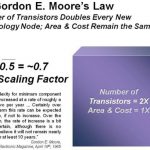
  • Moore’s Law and 40nm Yield
  • TSMC 40nm Yield Explained
  • EDA Marketing Fail TSMC Process Variation

Process variation really kicked in at 40nm and those that prepared yielded, those that didn’t, didn’t, simple as that. The process models had variation built into them but the main stream EDA tools did not. So Jen-Hsun was right, there was a major breakdown between the models and the tools. The reality breakdown however was a design management issue within Nvidia, which Jen-Hsun acknowledged in the interview.
The other news from Taiwan is the departures of Fu-Cheih Hsu and S.T. Juang from the TSMC Design and Technology Platform unit, founders of the TSMC Open Innovation Platform (OIP). EETimes broke the story on 9/20/2010 with “TSMC’s Design Guru Resigns”. Fu-Cheih actually left in August (typical mainstream media lag) with S.T. Juang following him in September.

I’ve received a lot of emails on this from vendors and customers alike. The big question is: will the TSMC OIP initiative continue? The answer of course is: YES it will. Fu-Cheih’s replacement is Cliff Hou who is even more qualified to advance the OIP agenda. Cliff is much more approachable, easy to work with, and has more “hands-on” semiconductor design enablement experience.

Cliff joined TSMC in Dec 1997 as a section manager responsible for process design kit (PDK) and reference flow development from 0.35m to 65nm. In 2007 Cliff became senior director of TSMC in-house IP development. TSMC IP includes: standard cells, IO’s, embedded memory compilers, analog blocks, and high-speed interface modules. He has a B.S. degree from National Chiao-Tung University, and a Ph.D. from Syracuse University, New York. He is also a member of the board of directors of Global Unichip Corp. Cliff knows semiconductor design enablement, absolutely.


TSMC Open Innovation Platform Explained

TSMC Open Innovation Platform Explained
by Daniel Nenni on 11-09-2009 at 10:56 pm

Launched in April 2008, the TSMC Open Innovation Platform initiative is a collaborative strategy aimed at breaking the bottlenecks of semiconductor design enablement in order to promote growth for the industry as a whole. The TSMC iPDK Debate: Lets Play Monopoly! blog I did provides more technical detail.

While Wafer count is climbing, an estimated 20M in 2009 to 30M in 2013, semiconductor design enablement (includes Electronic Design Automation-EDA, Semiconductor Intellectual Property-IP, and Design Services-DS) will continue to stagnate and consolidate.

The main reason for the disjointed wafer count increase and design enablement revenue stalling is FPGAs. As programmable devices advance in speed and density, medium-to-small volume projects and emerging technology companies will continue to leverage the low barrier to entry of FPGAs. Wafer count climbs from FPGA vendors such as Xilinx, Altera, and Actel, while ASIC design starts decline.
Other reasons for the ASIC design start decline include:

  • High cost, it takes $50-70M to get an ASIC to market.
  • Increased SOC design density and complexity, the chips are bigger so there are less of them and require many more resources to complete.
  • High mortality rate, an estimated 50% of the ASIC design starts do not make it into production.
  • Less ASIC design starts equals less design experience, less design experience equals higher ASIC mortality rate.


The TSMC Open Innovation Platform promotes timeliness-driven innovation amongst the semiconductor design community, its ecosystem partners and TSMC’s IP, design implementation and DFM capabilities, process technology and backend services. The Open Innovation Platform™ includes a set of ecosystem interfaces and collaborative components initiated and supported by TSMC that efficiently empowers innovation throughout the supply chain and enables the creation and sharing of newly created revenue and profitability. TSMC’s AAA initiative is a critical part of the Open Innovation Platform™, providing the accuracy and quality required by ecosystem interfaces and collaborative components.

The financial goal of OIP is obvious, to reduce waste in the semiconductor design enablement supply chain. People in this industry are accustomed to waste, business as usual, so this is a significant challenge! Jack Harding of eSilicon estimates a 20% waste due to inefficiencies and lack of experience. I say it is closer to 30% if you include the ASIC mortality rate. 20-30% of $50-70M is a significant amount, especially if you are asking a VC for it.

The TSMC OIP targets include the following areas of inefficiencies:

  • PDKs, the iPDK standard is innovation driven versus format driven, which reduces foundry and customer support costs.
  • EDA Reference Flows and tool qualification, verified design sign-off flows reduce both costs and customer learning curves.
  • TSMC IP portal, documenting silicon proven IP from both TSMC and commercial IP vendors such as Virage Logic. Cross distribution deals are also possible.
  • TSMC collaborated services, such as Tela Innovations Power and Area Trim.


The bottom line is that to increase ASIC design starts we must decrease the barrier to entry, we must reduce risk, we must all focus on success based business models:

  • TSMC is certainly success based with wafer pricing but must look at reducing NRE (mask costs) which are in the millions of dollars.
  • IP companies are success based capable with foundry sponsored IP (free to customers), and royalty based IP, but there are still significant up-front licensing fees for leading edge products.
  • Design Services (eSilicon) are definitely success based with per chip pricing for working silicon.
  • EDA is still in the dark ages with yearly subscriptions or all-you-can eat product dump pricing where you pay whether you use it or not, whether you are successful or not.

This was the second OIP conference, it was stocked with executives from TSMC and the design enablement food chain. The keynotes, panels, and discussions were highly interactive, the format and content is exactly what our industry needs to scale and move forward in a profitable manner.


TSMC versus SMIC

TSMC versus SMIC
by Daniel Nenni on 09-29-2009 at 12:24 am

This blog is about the legal battle between TSMC and SMIC which is currently playing in the California court system. Taiwan Semiconductor Manufacturing Corporation (TSMC) and Semiconductor Manufacturing International Corporation (SMIC) do what their names suggest – the manufacturing of semiconductors for an international roster of clients. TSMC touts itself as the first chip foundry, SMIC touts itself as the first China-based chip foundry. TSMC is ranked #1 , SMIC is #4, see my blog TSMC vs Global Foundries for more details on capacity and revenues.

The starting point is illustrated above, where SMIC went from equipment being installed in August of 2001, to qualified production in December 2001. As a point of proof, TSMC referred to the Fab of the Year Award that SMIC received from Semiconductor International in 2003, highlighting the fact that just four months after installing equipment in its fab, SMIC had four processes up and running, manufacturing 18 different products. Adding to that suspicion was the claim that SMIC hired away 100+ TSMC employees that had access to the sensitive process data required to bring a fab to production. To begin the legal discovery process, TSMC analyzed SMIC .18m silicon from a Broadcom product and documented stark similarities to the identical product silicon from TSMC. With discovery came incriminating emails which are a centerpiece of the case.

December 2003, TSMC filed suit alleging systematic intellectual-property (IP) theft and patent infringement by SMIC. Witness testimony indicated:

  • An estimated 90% of SMIC’s 180nm logic process was copied from TSMC
  • SMIC attempted to disguise the origin of the information by internally referring to TSMC and its technology by the code name ‘BKM1′, referring to ‘Best Known Method 1
  • SMIC’s use of TSMC technologies was ‘no secret’ and was openly discussed by SMIC engineers

Email supporting this testimony included exchanges between SMIC COO Marco Mora (a fromer TSMC employee) and then TSMC employee, Katy Liu, asking that she transfer TSMC’s process recipe documents and technical training manuals to SMIC. Proving once again, even very smart people can do very stupid things.

Not surprisingly, SMIC agreed to settle the case in February of 2005. Under terms of the settlement, SMIC is to pay TSMC $175 million over 6 years and the companies have agreed to cross license 180nm patent portfolios through December 2010.

In August 2006 TSMC filed a new lawsuit for more than $130 million alleging breach of the 2005 agreement. TSMC claims: SMIC continued copying TSMC manufacturing technology for newer (130nm) manufacturing processes in SMIC’s fabs, it also developed the advanced 90nm process using TSMC’s know-how.

“SMIC has carried out massive corporate espionage directed by certain [of] SMIC’s top operating officers,” the 31-page complaint said. “SMIC lavishly copied the information it stole from TSMC, word for word, line for line, diagram for diagram, and even typographical error for typographical error.”

In November 2006the High Court in Beijing accepted SMIC’s filing in which it claimed TSMC had intentionally disseminated untrue and misleading statements to damage SMIC’s reputation and goodwill.

TSMC “rather than competing fairly in the marketplace, have undertaken a concerted effort to infringe SMIC’s legal rights unfairly,”

TSMC filed in California for a reason, California has significant case law in regards to protecting intellectual property. SMIC filed in Bejing for a reason, China has scant case law in regards to intellectual property. It will be interesting how the Bejing and the California court proceedings compare. The California trial, which began this month, is expected to last 50-60 days, and is being broadcast by the Courtroom View Network. Trial updates will be available via my Twitter: DanielNenni


TSMC Versus Global Foundries

TSMC Versus Global Foundries
by Daniel Nenni on 09-13-2009 at 11:46 am

The big news last week was Global Foundries’ (GFI) agreement to acquire Chartered Semiconductor (CHRT) for $3.9B, but what does it really mean to the semiconductor world in total?

CurrentlyTSMC has 11 fabs producing wafers, 8 in Taiwan, 1 in Shanghai, 1 in Singapore, and 1 in Washington State. After the acquisition, Global Foundries will have Chartered’s 6 fabs in Singapore, AMD’s fab in Dresden with 1 more fab under construction in Dresden and another under construction in upstate New York, so 9 fabs in total.UMC has 10 fabs, 8 in Taiwan, 1 in Japan, and 1 in Singapore, and SMIC has control of 11 fabs in China. The ranking numbers above are clearly disjointed, UMC is #2 with 10 fabs, while SMIC is #4 with 11 fabs?

Unfortunately capacity does not guarantee economies of scale: TSMC owns 50% of the foundry market revenue and 80% of the profits, UMC is second with 12%, GFI, SMIC, and CHRT have yet to show a profit. Why are these numbers disjointed you ask? Wafer yield (good die per wafer) is important of course, yield is secret however, but from personal experience, TSMC is the top yielding foundry and these numbers support that.

Just as important is foundry wafer pricing, which, interestingly enough, is determined by the customer, more often than not. TSMC is considered a first source for semiconductor manufacture, UMC, CHRT, and SMIC are considered second sources, meaning that leading fabless semiconductor companies work with TSMC first, then replicate manufacturing at the other foundries. TSMC has the most advanced process technologies and the most skilled people so they are an easy first choice, reducing the risk of introducing a new product, and getting it to market as early as possible. Once the product is ramped on a TSMC process, wafer price becomes the central issue and the cutthroat negotiation with other fabs begin. Second and third sourcing also has fault tolerance built in, just in case Taiwan has a natural or unnatural disaster.

The foundry business challenge is to make their manufacturing processes sticky, focusing on customer retention, enabling a premium pricing strategy. Believe me, this is a key part of TSMC’s overall corporate strategy, a very deep customer loyalty program. Examples include:

  • Semiconductor design enablement programs, TSMC spends millions of dollars every year ensuring Semiconductor Design and Manufacture Predictability.
  • TSMC has a closely coupled services group in Global Unichip Corporation, which competes with the fabless ASIC companies mention in my blog: EDA is Dead.

Can GFI compete head-to-head with TSMC? Not now, and probably not ever. GFI’s United Arab Emirates based financial backing is a key selling point, deja vu of SMIC which is backed by the Chinese government but has yet to show a profit. GFI’s competitive advantage today is that they are not TSMC, for those who fear a foundry monopoly. Who knows what tomorrow will bring but based on my knowledge of the GFI executive staff, expect an innovative and sticky approach to the foundry business.