This is the first of a multi-part series, to introduce FinFET technology to SemiWiki readers. These articles will highlight the technology’s key characteristics, and describe some of the advantages, disadvantages, and challenges associated with this transition. Topics in this series will include FinFET fabrication, modeling, and the resulting impact upon existing EDA tools and flows. (And, of course, feedback from SemiWiki readers will certainly help influence subsequent topics, as well.)
Scaling of planar FET’s has continued to provide performance, power, and circuit density improvements, up to the 22/20nm process node. Although active research on FinFET devices has been ongoing for more than a decade, their use by a production fab has only recently gained adoption.
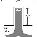
The basic cross-section of a single FinFET is shown in Figure 1. The key dimensional parameters are the height and thickness of the fin. As with planar devices, the drawn gate length (not shown) separating the source and drain nodes is a “critical design dimension”. As will be described in the next installment in this series, the h_fin and t_fin measures are defined by the fabrication process, and are not design parameters.
Figure 1. FinFET cross-section, with gate dielectric on fin sidewalls and top, and bulk silicon substrate
The FinFET cross-section depicts the gate spanning both sides and the top of the fin. For simplicity, a single gate dielectric layer is shown, abstracting the complex multi-layer dielectrics used to realize an “effective” oxide thickness (EOT). Similarly, a simple gate layer is shown, abstracting the multiple materials comprising the (metal) gate.
In the research literature, FinFET’s have also been fabricated with a thick dielectric layer on top, limiting the gate’s electrostatic control on the fin silicon to just the sidewalls. Some researchers have even fabricated independent gate signals, one for each fin sidewall – in this case, one gate is the device input and the other provides the equivalent of FET “back bias” control.
For the remainder of this series, the discussion will focus on the gate configuration shown, with a thin gate dielectric on three sides. (Intel denotes this as “Tri-Gate” in their recent IvyBridge product announcements.) Due to the more complex fabrication steps (and costs) of “dual-gate” and “independent-gate” devices, the expectation is that these alternatives will not reach high volume production, despite some of their unique electrical characteristics.
Another fabrication alternative is to provide an SOI substrate for the fin, rather than the bulk silicon substrate shown in the figure. In this series, the focus will be on bulk FinFET’s, although differences between bulk and SOI substrate fabrication will be highlighted in several examples.
Figure 2. Multiple fins in parallel spaced s_fin apart, common gate input
Figure 2 illustrates a cross-section of multiple fins connected in parallel, with a continuous gate material spanning the fins. The Source and Drain nodes of the parallel fins are not visible in this cross-section – subsequent figures will show the layout and cross-section view of parallel S/D connections. The use of parallel fins to provide higher drive current introduces a third parameter, the local fin spacing (s_fin).
Simplistically, the effective device width of a single fin is: (2*h_fin + t_fin), the total measure of the gate’s electrostatic control over the silicon channel. The goal of the fabrication process would be to enable a small fin spacing, so that the FinFET exceeds the device width that a planar FET process would otherwise provide:
s_fin < (2*h_fin + t_fin)
Subsequent discussions in this series will review some of the unique characteristics of FinFET’s, which result in behavior that differs from the simple (2*h + t) channel surface current width multiplier.
The ideal topology of a “tall, narrow” fin for optimum circuit density is mitigated by the difficulties and variations associated with fabricating a high aspect ratio fin. In practice, an aspect ratio of (h_fin/t_fin ~2:1) is more realistic.
One immediate consequence of FinFET circuit design is that the increments of device width are limited to (2h + t), by adding another fin in parallel. Actually, due to the unique means by which fins are patterned, a common device width increment will be (2*(2h+t)), as will be discussed in the next installment in this series.
The quantization of device width in FinFET circuit design is definitely different than the continuous values available with planar technology. However, most logic cells already use limited device widths anyway, and custom circuit optimization algorithms typically support “snapping” to a fixed set of available width values. SRAM arrays and analog circuits are the most impacted by the quantized widths of FinFET’s – especially SRAM bit cells, where high layout density and robust readability/writeability criteria both need to be satisfied.
The underlying bulk silicon substrate from which the fin is fabricated is typically undoped (i.e., a very low impurity concentration per cm**3). The switching input threshold voltage of the FinFET device (Vt) is set by the workfunction potential differences between the gate, dielectric, and (undoped) silicon materials.
Although the silicon fin impurity concentration is effectively undoped, the process needs to introduce impurities under the fin as a channel stop, to block “punchthrough” current between source and drain nodes from carriers not controlled electrostatically by the gate input. The optimum means of introducing the punchthrough-stop impurity region below the fin, without substantially perturbing the (undoped) concentration in the fin volume itself, is an active area of process development.
Modern chip designs expect to have multiple Vt device offerings available – e.g., a “standard” Vt, a “high” Vt, and a “low” Vt – to enable cell-swap optimizations that trade-off performance versus (leakage) power. For example, the delay of an SVT-based logic circuit path could be improved by selectively introducing LVT-based cells, at the expense of higher power. In planar fabrication technologies, multiple Vt device offerings are readily available, using a set of threshold-adjusting impurity implants into masked channel regions. In FinFET technologies, different device thresholds would be provided by an alternative gate metallurgy, with different workfunction potentials.
The availability of multiple (nFET and pFET) device thresholds is a good example of the tradeoffs between FinFET’s and planar devices. In a planar technology, the cost of additional threshold offerings is relatively low, as the cost of an additional masking step and implant is straightforward. However, the manufacturing variation in planar device Vt’s due to “channel random dopant fluctuation” (RDF) from the implants is high. For FinFET’s, the cost of additional gate metallurgy processing for multiple Vt’s is higher – yet, no impurity introduction into the channel is required, and thus, little RDF-based variation is measured. (Cost, performance, and statistical variation comparisons will come up on several occasions in this series of articles.)
The low impurity concentration in the fin also results in less channel scattering when the device is active, improving the carrier mobility and device current.
Conversely, FinFET’s introduce other sources of variation, not present with planar devices. The fin edge “roughness” will result in variation in device Vt and drive current. (Chemical etch steps that are selective to the specific silicon crystal surface orientation of the fin sidewall are used to help reduce roughness.)
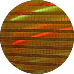
The characteristics of both planar and FinFET devices depend upon Gate Edge Roughness, as well. The fabrication of the gate traversing the topology over and between fins will increase the GER variation for FinFET devices, as shown in Figure 3.
Figure 3. SEM cross-section of multiple fins. Gate edge roughness over the fin is highlighted in the expanded inset picture. From Baravelli, et al, “Impact of Line Edge Roughness and Random Dopant Fluctuation on FinFET Matching Performance”, IEEE Transactions on Nanotechnology, v.7(3), May 2008.
The next entry in this series will discuss some of the unique fabrication steps for FinFET’s, and how these steps influence design, layout, and Design for Manufacturability: